Regarding layout: It mostly boils down to knowing that there are stray impedances. Where on a circuit diagram two components are joined by a line, in reality it's actually a resistance and inductance. Also there are capacitances between components. You need to be aware of what effect these will have and design to minimize their effects.
For instance, even a very small inductance in the source or drain of a MOSFET can send it into oscillation, so you must make sure that those tracks are as short as possible. Also place supply bypass capacitors as close to the circuit as possible (there don't seem to be any in the amp posted here, but I would recommend using some anyway, just to be safe), again to minimize the effects of inductance.
Grounding is a major area of concern. You may have a track which you call ground, but since it will have a finite impedance, any current flowing in it will raise its potential above what you would like it to be, which can inject hum and noise into anything grounded there. Using a star-ground and keeping high current and noisy grounds separate helps a lot.
Other things to consider include heat and EMI, ease of construction, fault conditions etc, but whole books could be written on the subject.
Thank you for reply Mr Evil.
Think I know what you mean, there is both capacitive and inductive behavior of a pcb and coupling between components on a PCB. I was looking at the pcb of the amp in this thread and stargrounding was used as well as short tracks but no bypass caps on the psu rail. As you said, this is a real big subject and it can not be explaned even in a pile of A4 sheet. I'll try to find some books about how to route pcb:s
Since this thread started with thermal compensation on mosfet amps I will stop here. Anyhow, it would be interesting to post a schematic in a new thread and let some experts make their own layouts and post them as well, just to see the difference.
Bjorn

Hello B.I.G!
Sometimes I see comments like: this board will not work it will oscillate or be noisy. I know that if you don't have proper knowledge in fundamentals about components involved and what makes inductive and capacitive components on a pcb it will not be an easy task to explane and can not be compressed in a few rows of text.
We could choose any amp maybe two, one with BJTs and one with FETs and just to make it simple enough a small number of components so it can be explaned as simple as possible.
There are lot's of books written on almost any subject wich comes up on DIY so why not pcb design?
Excuse me for repeating my self a little and for being off topic but since the question came...
Am I way out of....?
Bjorn
Thank you jacco vermeulen!
Sorry for doing this again I mean using B.I.Gs thread for another purpose even tough for a short while.
It's hard to come up with something good about the title.
Maybe a title for a new thread would be: PCB routing for audioamps?
It must be clear that it is in no way any sort of competiton.
Bjorn
Sorry for doing this again
I mean using B.I.Gs thread for another purpose even tough for a short while.It's hard to come up with something good about the title.
Maybe a title for a new thread would be: PCB routing for audioamps?
It must be clear that it is in no way any sort of competiton.
Bjorn
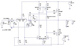
B.I.G said:would this circuit work ? i see no thermal compesation ..... so wouldnt it blow the output devices ? i see the author recomending irfp240/9240 that are not lateral devices.....
http://users.swing.be/edwinpaij/ampli_mosfet_simple.htm
I have built those amplifier.Works good.With little change-Mosfets are IRF640/9640, (at 4 ohm-two pairs) T3,4=MJE350, T5,T6=MJE340, T1,T2=2N5401. At V+/- MUST 100n 250V(not in shematic), P1=470R Fixed, power supply-65V.
I can recommend this shematic, it is cheap and works good and stable. here is photo of my PCB variant:
An externally hosted image should be here but it was not working when we last tested it.
An externally hosted image should be here but it was not working when we last tested it.
- Status
- This old topic is closed. If you want to reopen this topic, contact a moderator using the "Report Post" button.
- Home
- Amplifiers
- Solid State
- mos-fet amplifier question ...