This circuits also fascinates me.
But first - a short interruption. The author is Dutch. His first name is Wim and his surname is De Jager, not Jager. This translates into English as The Chaser, more or less.
Back to the circuit. Some of the devices, such as the matched pairs and output transistors used are now obsolete. Trying to simulate it is therefore a hassle as no models are to be found. I've tried...
However, I did manage to make a few substitutions and it works. The collector currents do indeed stay above zero, as advertised.
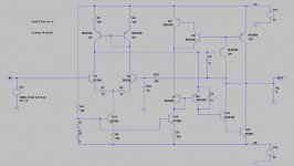
Here is my circuit with modern(!) devices and a plot of the collector currents in the output stage. It was done with LTspice IV. If there is any interest, I will post the LTspice file and the Spice models used.
The magic in this circuit lies in Q6, Q7, Q8 and Q9. Their base-emitter junctions form an uninterrupted loop, which makes it a translinear circuit. Through a bit of math, you come up with the equation
Ic6.Ic7 = Ic8.Ic9
With Ic8 related to Ic11 and Ic9 to Ic12, it becomes clear that they must all be non-zero for the above equation to hold. If anyone is interested, I can elaborate on the above math and on translinear circuits.
I would also like to know if this design has been used commercially. My guess is that it is not exactly cost efficient, as it uses a _lot_ of transistors for not a lot of watts. But then again, that should appeal to the flat earth brigade, hehehehe....
But first - a short interruption. The author is Dutch. His first name is Wim and his surname is De Jager, not Jager. This translates into English as The Chaser, more or less.
Back to the circuit. Some of the devices, such as the matched pairs and output transistors used are now obsolete. Trying to simulate it is therefore a hassle as no models are to be found. I've tried...
However, I did manage to make a few substitutions and it works. The collector currents do indeed stay above zero, as advertised.
Here is my circuit with modern(!) devices and a plot of the collector currents in the output stage. It was done with LTspice IV. If there is any interest, I will post the LTspice file and the Spice models used.
The magic in this circuit lies in Q6, Q7, Q8 and Q9. Their base-emitter junctions form an uninterrupted loop, which makes it a translinear circuit. Through a bit of math, you come up with the equation
Ic6.Ic7 = Ic8.Ic9
With Ic8 related to Ic11 and Ic9 to Ic12, it becomes clear that they must all be non-zero for the above equation to hold. If anyone is interested, I can elaborate on the above math and on translinear circuits.
I would also like to know if this design has been used commercially. My guess is that it is not exactly cost efficient, as it uses a _lot_ of transistors for not a lot of watts. But then again, that should appeal to the flat earth brigade, hehehehe....
Attachments
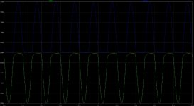
I think I have found the reason that the design never caught on. A Fourier analysis on LTspice shows a THD of about 0.3% - not exactly ground breaking. It may well be that TIM is quite good but I have not investigated that. The 'high' THD may be caused by both transistors being on all the time. In his book Douglas Self goes on about the perils of class AB. Perhaps this design falls into that trap and in trying to solve one problem (switching distortion) it makes another one worse. Does anybody have any thoughts on the matter?
Here's one (below) . They last 20 years and sound real good. D701 / 703 are geraniums. These simulated well sub'ed with schottky diode's . Just 4 transistors makes for the Vbe and the non-switching OPS. Circuit idles OP's at about 10ma (never shuts them off - "krill like").
PS- I have the real thing to reverse engineer (actually 2 of them).
Another way to get low Xover is to use either a "fancy Vbe" or thermaltraks.
OS
PS- I have the real thing to reverse engineer (actually 2 of them).
Another way to get low Xover is to use either a "fancy Vbe" or thermaltraks.
OS
Attachments
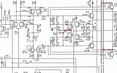


This is Nikko amp. Germanium are diodes D701 / 703, just for small voltage drop.
What?

It is my own design, circa 1978.
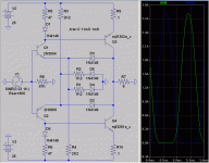
In the schematic by post #22 I miss resistors in parallel to the base and emitter connectors of Q11 and Q12.
That means, the idle current through Q9 and Q10 was only determined by the idle current (and thus the base input current) through Q11 and Q12.
The same situation is to find by Q6, because the resistor in parallel to B-E of Q5 is also not present.
What means the sacrifice of this resistors?
Naturally at this place is to find a resistor for exactly determine of this current value (independend of the base input current from follow second stage of the darlington - even in integrated darlingtons like BDX87C or BDX67C).
From the same authors I have find this:
http://ieeexplore.ieee.org/Xplore/l...6/00000320.pdf?arnumber=320&authDecision=-203
That means, the idle current through Q9 and Q10 was only determined by the idle current (and thus the base input current) through Q11 and Q12.
The same situation is to find by Q6, because the resistor in parallel to B-E of Q5 is also not present.
What means the sacrifice of this resistors?
Naturally at this place is to find a resistor for exactly determine of this current value (independend of the base input current from follow second stage of the darlington - even in integrated darlingtons like BDX87C or BDX67C).
In the meantime this URL is death. Are there a new URL with same pages?Thank you very much for this URL:
http://home.tiscali.nl/data.odyssey/files/Jager/
do you know commercial amps uses this topology and that one mentioned by post #11?
From the same authors I have find this:
http://ieeexplore.ieee.org/Xplore/l...6/00000320.pdf?arnumber=320&authDecision=-203
Last edited:
From the same authors I have find this:
IEEE Xplore - Sign In
I have a scan of a photocopy of the above, complete with a few hand drawn alterations. The quality isn't great, but it is readable. Unfortunately, the file size of 1.26 MB bytes exceeds the forum's limit of 195.3 KB for PDF files. Can anybody suggest a suitable upload site where I can put it?
you can send it to me and I can try to convert it in a DOC-file (and then in a PDF file) aboutI have a scan of a photocopy of the above, complete with a few hand drawn alterations. The quality isn't great, but it is readable. Unfortunately, the file size of 1.26 MB bytes exceeds the forum's limit of 195.3 KB for PDF files. Can anybody suggest a suitable upload site where I can put it?
ABBYY FineReader 9.0 Pro.
My e-mail address: kirschner-hifi@tiefbassuebertragung.de
If you don't mind using a lot of extra transistors, you can pretty much force any relation you like between the output device currents by means of a non-linear common-mode loop, which to the best of my knowledge was first used by Johan H. Huijsing and Frans Tol in 1976 (see "Monolithic operational amplifier design with improved HF behavior", IEEE Journal of solid-state circuits, April 1976).
The general idea is that you somehow sense the output device currents, for example by small resistors in the output device leads. The sensed currents are then put into a non-linear circuit with two inputs and one output, where the output is mainly sensitive to the smallest of the two input quantities. A feedback loop then tries to make the output of the non-linear circuit equal to some set value. This feedback loop increases or decreases the currents through both output devices simultaneously and therefore does not affect the output current of the amplifier.
Huijsing and Tol used a multiplier as the non-linear circuit, I used the sum of two exponential functions (exp(-K*I1)+exp(-K*I2), see Electronics World February 1996), others have used harmonic mean functions.
Class AB new driver stage EW pg 982-985
Obviously I have save this site, that I have forget by the last post. I have do a splitting and converted to PDF files. Thus sending via e-mail to my address isn't longer necessary.you can send it to me and I can try to convert it in a DOC-file (and then in a PDF file) about
ABBYY FineReader 9.0 Pro.
My e-mail address: kirschner-hifi@tiefbassuebertragung.de
Attachments
-
Class AB new driver stage EW pg 983-I.pdf56.3 KB · Views: 411
-
Class AB new driver stage EW pg 982-II.pdf110.3 KB · Views: 428
-
Class AB new driver stage EW pg 982-I.pdf102.4 KB · Views: 510
-
Class AB new driver stage EW pg 983-II.pdf88.5 KB · Views: 329
-
Class AB new driver stage EW pg 983-III.pdf59.5 KB · Views: 289
-
Class AB new driver stage EW pg 984-I.pdf91.2 KB · Views: 288
-
Class AB new driver stage EW pg 984-II.pdf84.3 KB · Views: 307
-
Class AB new driver stage EW pg 985-I.pdf60.6 KB · Views: 312
-
Class AB new driver stage EW pg 985-II.pdf123.6 KB · Views: 375
Last edited:
- Home
- Amplifiers
- Solid State
- low crossover-distortion class AB output stage topologies