The JVC AX-M9000 Monaural Integrated Amplifier was quite a concept. Never saw anything like it. Does anybody know more about it? When was it available? Was it replaced by something similar or was the idea a commercial dead end?
Google only dishes up websites that claims to have the service manual - dozens and dozens of them.
Google only dishes up websites that claims to have the service manual - dozens and dozens of them.
That chip looks like an early version of the LT1166 http://cds.linear.com/docs/Datasheet/lt1166.pdf which does the same thing.
The secret is in the internal exponential gain curve.
There's a thread here somewhere on the chip.
jan didden
Is anyone using the 1166 in a production amplifier?

No! - ohh maybe Linn!? ha ha ha.
Back to the drawing board. Nothing comes for free.
But Mosfet... Actually - I think i have sold my old love, the BJT to use Mosfet instead.
Much, much easier to get stable.. And then we can fool around trying to reduce the crossover region.
The only feedbackless functions that result in no distortion are: linear class A,
and complementary square laws class A, or any weighted blend of these two.
Neither curve, or any inbetween, offers us the low quiescent we might want.
Choose any other curve for lower quiescent, and crossing distortion is certain.
Therefore needs very fast, direct coupled, local error correction. Independent
of the global loop. If the error is corrected, we can abuse any curve we wish.
I'm not intending to contradict anyone, just clarifying a point thats sometimes
not so self-evident the first time one looks at existing systems to achieve it.
I sure didn't get Hawksford the first time I saw it...
Hi Peter;
what about this one?
http://www.diyaudio.com/forums/atta...n-class-ab-output-stage-topologies-nuclon.gif
The idea was, if you remember, to use diodes to shift between lower power class A and higher power class B, instead of using starved output devices themselves.
what about this one?
http://www.diyaudio.com/forums/atta...n-class-ab-output-stage-topologies-nuclon.gif
The idea was, if you remember, to use diodes to shift between lower power class A and higher power class B, instead of using starved output devices themselves.
I remember redrawing that for you, was impressive...
If I recall, it had shorted output current limiting too?
But corrects output V to match input V with a relatively long leash.
Perhaps if D2 and D3 were transistor drops that match Q1 and Q2?
Then again, transistors would be a messy shutoff in B crossing.
If I recall, it had shorted output current limiting too?
But corrects output V to match input V with a relatively long leash.
Perhaps if D2 and D3 were transistor drops that match Q1 and Q2?
Then again, transistors would be a messy shutoff in B crossing.
Last edited:
If D2 and D3 would be transistors it would turn into a complementary opamp. The trick is in tails of diffstages. They are normally biased in class A, for higher load resistance / lower power, but when output goes from zero additional diodes D4 and D5 in tails open to add more current for class B operation. And yes, if to short outputs D2 and D3 would close turning the amp into current output mode. Transistors in place of D2 and D3 would not cause messy shutoff in B crossing. They would be fried due to limited base-emitter breakdown voltage when output is shorted.
Member
Joined 2009
Paid Member
I remember simulating it, and in my simulations I found that it relies on plenty of nfb to keep distortion under control ?
Like any other follower.
But it does not use feedback to correct cross-over distortions of starved output devices, this is the main point! Output devices don't starve in cross-over point, they always operate. They starve on peaks, when an opposite device saturates, exactly like in case of classical class A mode.
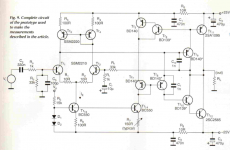
i found equivalent circuit diagram of JVC's super A circuit IC "VC5022".
JVC AXM9000E Service Manual free download,schematics,datasheets,eeprom bins,pcb,repair info for test equipment and electronics
by post #2542 about
????????? ?????? ?? ?. ??????? - ????? ?? ???????????????? - ???????? 127,5
I have found explicit VC5022 circuit (JVC VC5022 circuit for a discrete clone).
Attachments
Is anyone using the 1166 in a production amplifier?
I don't know single power/integrated amplifier components. I think, this IC is used in so called "hifi Systems" with adjustmnent free power amp sections and thus the according models are very hard zu find.
The follow keywords
""LT1166" and "Service Manual" for Google unfortunately provides no results
Last edited:
Non-Switching Class AB
The New Class AB design from Erik van der Veen and Ed van Tuyl (Electronics World, december 1999) was mentioned in Post #13, 22 +...
The original article can be found at https://andiha.no/audio/temp/newclassab.pdf
A closer look at the design made me think it would be possible to improve the design.
In spite of the high open loop gain, the distortion is rather high and both the open loop bandwidth and slew rate is rather low.
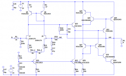
The original design schematic is shown here.
The New Class AB design from Erik van der Veen and Ed van Tuyl (Electronics World, december 1999) was mentioned in Post #13, 22 +...
The original article can be found at https://andiha.no/audio/temp/newclassab.pdf
A closer look at the design made me think it would be possible to improve the design.
In spite of the high open loop gain, the distortion is rather high and both the open loop bandwidth and slew rate is rather low.
The original design schematic is shown here.
Attachments
New Class AB design - Build this?
My proposal is shown. The main improvement is the added emitter follower. This both reduces the distortion significantly and makes it possible to increase the slew rate figure and the open loop bandwidth.
I am a fan of using JFET input transistors, eliminating the input coupling capacitor.
Simulation looks promising, so the question is:
Would someone try to build it?
I am to busy to do it myself, I am afraid...
Attachments
New Class AB design - Build this?
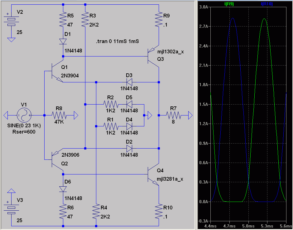
Here is my LTSpice file. R11 is the offset adjustment and R25 is the bias adjustment.
The distortion is less than 0.01 % at 25 W into 8 ohms with a bias of 0.6 Ampere. Then the collector current for the output transistors is more than 40 mA minimum. However, if the bias current is lower, the distortion rises heavily and the output transistors is nearly switched off (and I don't know the reason why).
The open loop gain is about 56 dB with a bandwidth of about 20 kHz. The phase margin is more than 80 degrees.
Attachments
Last edited:
- Home
- Amplifiers
- Solid State
- low crossover-distortion class AB output stage topologies