Class AB new driver stage EW pg 986-987
... and the last two pages of this amplifier project from ELECTRONICS WORLD December 1999:
... and the last two pages of this amplifier project from ELECTRONICS WORLD December 1999:
Attachments
-
Class AB new driver stage EW pg 986-I.pdf116.6 KB · Views: 359
-
Class AB new driver stage EW pg 986-II.pdf90.1 KB · Views: 283
-
Class AB new driver stage EW pg 987-I.pdf76.3 KB · Views: 285
-
Class AB new driver stage EW pg 987-II.pdf74.4 KB · Views: 286
-
Class AB new driver stage EW pg 987-III.pdf110.8 KB · Views: 300
Last edited:
You need good thermal tracking in the translinear loop Tr6-Tr7-Tr8-Tr9, but the output transistors are outside this loop. Only the temperature coefficient of the hFE of the output transistors affects the bias current, not their VBE shift with temperature. So I don't expect the temperature dependence to be that bad.
")
Three things must happen:
1) Quiescent current must never run away.
1) Shutoff into B must be tempered with a gentle knee
1) Strong local feedback must correct crossover distortion.
Any feedback-less crossing not based upon linear law class A,
and/or complimentary square law class A will probably distort.
But you can combine these two in any proportion and have
a crossing that does not distort. But might not have quite as
low a quiescent as you'd like. Going lower means accepting
local distortion and applying local correction for it.
No comments?In the schematic by post #22 I miss resistors in parallel to the base and emitter connectors of Q11 and Q12.
That means, the idle current through Q9 and Q10 was only determined by the idle current (and thus the base input current) through Q11 and Q12.
The same situation is to find by Q6, because the resistor in parallel to B-E of Q5 is also not present.
What means the sacrifice of this resistors?
Naturally at this place is to find a resistor for exactly determine of this current value (independend of the base input current from follow second stage of the darlington - even in integrated darlingtons like BDX87C.
By the PDF file "Class AB new driver stage EW pg 985-I" about post #40 is Q = Tr
Last edited:
the other topology was in little vogue in japanese DIY scene since some years ago.
like yamaha's HCA circuit
ex.
Trans_linear_Bias
TLB_2SJ200/2SK1529PowerAmp
‚QSK1529/2SJ200MonauralPowerAmplifier
2SK3497/2SJ618PowerAmplifier
please use translation tool...
like yamaha's HCA circuit
ex.
Trans_linear_Bias
TLB_2SJ200/2SK1529PowerAmp
‚QSK1529/2SJ200MonauralPowerAmplifier
2SK3497/2SJ618PowerAmplifier
please use translation tool...
Shinja, I like the first of your references. Looks like a whole bunch of nice implementations of the Van Tol/Huijsing non-linear common-mode loop technique.
Tiefbassuebertr, the 1999 Electronics World circuit relies on the output transistors being more or less linear current amplifiers over a large current range. The idle current of Tr9 is supposed to be set by the translinear loop Tr6-Tr7-Tr8-Tr9 and the current through the output transistors is then simply hFE times greater. Connect resistors in parallel with the base-emitter junctions of Tr11 and Tr12 and the whole concept doesn't work anymore.
Of course this means that when you adjust the bias current of Tr14 until you have a certain desired current through Tr11 and Tr12, then the bias of Tr9 is rather unpredictable as it depends on the hFE of the output transistors, which is generally not an accurately known parameter.
The situation is even worse for Tr6 and Tr7. Within the translinear loop, ITr7*ITr6*IsPNP/IsNPN=ITr8*Itr9, with IsPNP/IsNPN=exp(q(VBENPN-VBEPNP)/kT). That is, the required bias current through Tr6 and Tr7 that is needed to get a given current through Tr8 and Tr9 changes by roughly a factor of three when you have 60 mV of VBE mismatch between two unequal devices, an NPN and a PNP.
Best regards,
Marcel
As promised, here is the paper by Seevinck e.a. from the IEEE Journal of Solid-state Circuits Vol 23 No.3
Attachments
And the last two pages.
Page 800 had to be converted to a picture because of file size restrictions.Maybe that's what I should have done from the start.
Anyway - enjoy the article. It is quite scholarly. Once again, apologies for the quality.
Page 800 had to be converted to a picture because of file size restrictions.Maybe that's what I should have done from the start.
Anyway - enjoy the article. It is quite scholarly. Once again, apologies for the quality.
Attachments
Hi ingenieus,
Yes, that is THE classical article on harmonic mean class AB loops. For an almost discrete design, it is much easier to make something like exp(-K*I1)+exp(-K*I2), rather than a harmonic mean. Choose K properly and you get a quite similar current distribution between the positive and negative sides, but which much fewer matched transistors (only four, plus four resistors).
Best regards,
Marcel
Attachments
This URL's are a great source for circuit ideas - thank you therefore.the other topology was in little vogue in japanese DIY scene since some years ago.
like yamaha's HCA circuit
ex.
Trans_linear_Bias
TLB_2SJ200/2SK1529PowerAmp
‚QSK1529/2SJ200MonauralPowerAmplifier
2SK3497/2SJ618PowerAmplifier
please use translation tool...
Which circuit is like Yamaha's HCA topology? - go to post #40 about
http://www.diyaudio.com/forums/soli...c-conversion-amplification-hca-circuit-4.html
for simplifield schematic.
Thank you for this explanations.Shinja, I like the first of your references. Looks like a whole bunch of nice implementations of the Van Tol/Huijsing non-linear common-mode loop technique.
Tiefbassuebertr, the 1999 Electronics World circuit relies on the output transistors being more or less linear current amplifiers over a large current range. The idle current of Tr9 is supposed to be set by the translinear loop Tr6-Tr7-Tr8-Tr9 and the current through the output transistors is then simply hFE times greater. Connect resistors in parallel with the base-emitter junctions of Tr11 and Tr12 and the whole concept doesn't work anymore.
Of course this means that when you adjust the bias current of Tr14 until you have a certain desired current through Tr11 and Tr12, then the bias of Tr9 is rather unpredictable as it depends on the hFE of the output transistors, which is generally not an accurately known parameter.
The situation is even worse for Tr6 and Tr7. Within the translinear loop, ITr7*ITr6*IsPNP/IsNPN=ITr8*Itr9, with IsPNP/IsNPN=exp(q(VBENPN-VBEPNP)/kT). That is, the required bias current through Tr6 and Tr7 that is needed to get a given current through Tr8 and Tr9 changes by roughly a factor of three when you have 60 mV of VBE mismatch between two unequal devices, an NPN and a PNP. Best regards, Marcel
Last edited:
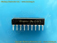
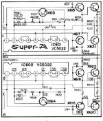
i found equivalent circuit diagram of JVC's super A circuit IC "VC5022".
JVC AXM9000E Service Manual free download,schematics,datasheets,eeprom bins,pcb,repair info for test equipment and electronics
JVC AXM9000E Service Manual free download,schematics,datasheets,eeprom bins,pcb,repair info for test equipment and electronics
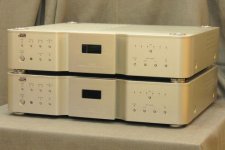
JVC AX-M9000 Monaural Integrated Amplifier use " Advanced Super A" Topology
Thank you very much for this advice.
There are a lot of mono power amplifier models, but integrated amplifiers in mono I have never see before.
This IC seems to be a custom made version, but the internal circuit is show.
Also some offers are to find online, e. g.
http://www.bluestar-online.com/VC5022_p/vc5022.htm?gclid=CPejvNyl6pECFSaSQAod1xMxYA
The front outline reminds me of Jeff Rowland (see attachement)
About
http://www.elektroda.pl/rtvforum/topic1220227.html (post from Oct., 26, 2009)
is to read, a replacement is follow:
http://www.datasheetcatalog.org/datasheet/sanyo/LA2500.pdf
i found equivalent circuit diagram of JVC's super A circuit IC "VC5022".
JVC AXM9000E Service Manual free download,schematics,datasheets,eeprom bins,pcb,repair info for test equipment and electronics
Thank you very much for this advice.
There are a lot of mono power amplifier models, but integrated amplifiers in mono I have never see before.
This IC seems to be a custom made version, but the internal circuit is show.
Also some offers are to find online, e. g.
http://www.bluestar-online.com/VC5022_p/vc5022.htm?gclid=CPejvNyl6pECFSaSQAod1xMxYA
The front outline reminds me of Jeff Rowland (see attachement)
About
http://www.elektroda.pl/rtvforum/topic1220227.html (post from Oct., 26, 2009)
is to read, a replacement is follow:
http://www.datasheetcatalog.org/datasheet/sanyo/LA2500.pdf
Attachments
-
JVC AX-M9000 IC302 Advanced Super A.pdf21.9 KB · Views: 265
-
JVC AX-M9000 Monaural Integrated Amp Cover SM.pdf54 KB · Views: 202
-
 JVC AX-M9000 Monaural Integrated Amplifier.jpg28.7 KB · Views: 808
 -
JVC AX-M9000 IC302 Advanced Super A power amp II.pdf131 KB · Views: 235
-
JVC AX-M9000 IC302 Advanced Super A power amp I.pdf116.9 KB · Views: 245
-
 JVC vc_5022-2-2.jpg138.4 KB · Views: 777
Last edited:
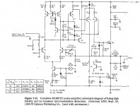
I have come across another circuit that claims to eliminate TIM. It is from the book "Power FETs and Their Applications" by Edwin S. Oxner (staff engineer, Siliconix Incorporated) published by Prentice-Hall, 1982. The ISBN is 0-13-686923-8.
The author describes it as follows on page 201-202:
In the diagram, the design is credited to an article that appeared in EDN on Sept. 20, 1980. I have not been able to locate this article on the interweb. Doing a SPICE simulation would be a challenge due to finding models for the obsolete parts. Perhaps an updated version with modern components can be brewed up.
All I can say is that it probably does not live up to the bold claims made for it, otherwise it would have been in wide use. Does anyone care to comment on the workability of this design?
The author describes it as follows on page 201-202:
A novel design using power MOSFETs is shown in Fig. 7-21.The novelty of this circuit stems from the action of the zener diodes, Z3, Z4 and Z5, which prevents the pnp bipolar transistors, Q10 and Q11, from conducting at any time their bases are driven positive by the signal. What we are witnessing is somewhat unusual for a power amplifier is Class AB1 operation, not in the final MOSFETs, but in the drivers. Rather than being simple differential amplifiers as we would find in most conventional designs, Q10 and Q11 have sufficient punch to handle the driving needs of the largest MOSFETs at high slew rates (i = C dV/dt). Note especially the low value of gate resistance for the power MOSFETs.
Because of the extraordinary wide open-loopbandwidth and high gain of this amplifier, transient intermodulation distortion is totally absent!
In the diagram, the design is credited to an article that appeared in EDN on Sept. 20, 1980. I have not been able to locate this article on the interweb. Doing a SPICE simulation would be a challenge due to finding models for the obsolete parts. Perhaps an updated version with modern components can be brewed up.
All I can say is that it probably does not live up to the bold claims made for it, otherwise it would have been in wide use. Does anyone care to comment on the workability of this design?
Attachments
Member
Joined 2009
Paid Member
things must happen:
1) Strong local feedback must correct crossover distortion.
Some people have found that the sound of certain Class AB amps is perfectly enjoyable without strong feedback correction (i.e. that aimed at reducing the cross-over distortion). There are a number of examples such as Steven Dunlap's KRILL.
- Home
- Amplifiers
- Solid State
- low crossover-distortion class AB output stage topologies