Hi everyone,
I've been reading these forums for a while now, and found quite a lot of help on my different projects. Right now, I'm stumped. And this is my first post here. I'm not expecting anyone to solve the problem(s) right off, and any help will be appreciated.
I have this Yamaha P-2200 amp (Priscared has posted a lot about this amp) and blew it up real good doing a stupid thing (connected both channels to the same speaker by mistake then tried to play loud).
Anyway, after bashing myself on the head for a week, I gathered the parts I needed to repair both channels, and I have just about everything.
I tested every part I could (resistors, caps, semis) and I found that a few fuse resistors and most semis from the predrive stage onward were gone (tr109 and up, plus two diodes), some even with vaporized portions. I rebuilt one channel from the good parts on both, and this is where I'm at.
Since the original devices from Yamaha are horribly expensive, I used 2N5551, 2N5401, MJE15032, MJE15033 as replacements, and will switch to MJ21193/4 for the outputs. Right now, I was able to recover enough pairs to rebuild this channel with the original SanKen, so this is what I'm testing.
Stage by stage, I was able to find that nothing was running away hot, but I definitely have a problem: there's approx. 10VDC at the center point, not 0. I tried to figure out why, but this circuit is too complex for me. I have the service manual (flimsy) and have read it through many times. I understand it superficially, but I wouldn't be able to analyze the circuit with the information given in there and modify/upgrade the circuitry. In a few years, probably.
The bias voltage is set to 11mV, the closest I can get it to Yamaha's recommended value, for what it's worth. The center voltage is taken between PE and E (see the right-side of the attached schematic).
The 13VAC supply is actually 11.7VAC, giving out 9.6VDC instead of the expected 11.4, so that screws up all indicated voltages on the bottom rail.
The voltages around TR107 are correct except for the collector which is at 40V instead of 44.3
At the bases of TR111 and TR112 there's about -10V instead of the expected +/- 1.2V. An aside here: when I replaced these two drivers with the MJE1503?s I could not get my hands on matched pairs. Does it matter in this type of design? The beta has a 2:1 ratio between the NPN/PNPs. Matching the 2N5551 & 2N5401 was easier.
Any ideas?
Thanks
Andre
Attachments
Hmm....
I'll have a closer look at the cct later but my initial thoughts are.
The input stage emitters of TR101 & 102 should be 0.6 volts (relative to gnd) if they aren't then this could be caused by the problem you described for the negative driver rail which should be -92 volts. This would explain the 10v on the output.
Disconnect the AC from the board and measure it. If it jumps to over 13VAC then something is loading it down. Is R134 hot? If it is then you have a problem to the left of it. If it isn't hot then check it for open circuit. If it measures 100 ohms then check the diode bridge rectifiers D114 & D115 while I (and others) look at the cct some more.
Cheers & good luck
I'll have a closer look at the cct later but my initial thoughts are.
The input stage emitters of TR101 & 102 should be 0.6 volts (relative to gnd) if they aren't then this could be caused by the problem you described for the negative driver rail which should be -92 volts. This would explain the 10v on the output.
The 13VAC supply is actually 11.7VAC, giving out 9.6VDC instead of the expected 11.4, so that screws up all indicated voltages on the bottom rail.
Disconnect the AC from the board and measure it. If it jumps to over 13VAC then something is loading it down. Is R134 hot? If it is then you have a problem to the left of it. If it isn't hot then check it for open circuit. If it measures 100 ohms then check the diode bridge rectifiers D114 & D115 while I (and others) look at the cct some more.
Cheers & good luck
Update
Thanks for those quick replies, guys!
Here's what I have checked so far this morning:
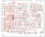
My supply rails are not perfectly symmetrical anymore: I now have a 1V difference: -81V and 80V. This has been happening since after I checked TR105 and 6 (matched), R126, D106-7 last night by taking them out and putting them back in (after the post). I don't know if this is significant. Before that, they were identical. Something else: since I adjusted the bias to 11mV, TR107 runs hotter. I've included a second picture, of the PCB this time.
Quasi:
The input stage emitters (TR101-2) are at -3.45V
The AC voltage is the same connected or not, stays around 11.3V.
R134 is not hot, and is precisely 100ohms
The rectifiers (D114-5) are operational
Djk:
Changed C106, no difference, will probably put back the original (110 deg Nippon Chemi-Con, very long life, ain't broke, don't fix). Actually, all the electrolytics are like that one, and none shows signs of wear.
R123,4,5 have 27mA running through them
R127 has 8.7mA
Those four resistors and TR107 are the only things running warm/hot. I never leave the amp on for more than a minute or two, just for taking measurements.
I also don't understand your comment (that's a little bit further than me). I am going through Slone's "Understanding Electronics" and "How to build high-power amps..." slowly, among a zillion other things. I'm at building transistor circuits to understand their behaviours under various conditions. Later.
Markp:
I haven't checked VR101, but I was able to adjust the bias properly (it seems). Do I need to go further? I'm trying to keep the soldering/desoldering to a minimum.
Thanks for those quick replies, guys!
Here's what I have checked so far this morning:
My supply rails are not perfectly symmetrical anymore: I now have a 1V difference: -81V and 80V. This has been happening since after I checked TR105 and 6 (matched), R126, D106-7 last night by taking them out and putting them back in (after the post). I don't know if this is significant. Before that, they were identical. Something else: since I adjusted the bias to 11mV, TR107 runs hotter. I've included a second picture, of the PCB this time.
Quasi:
The input stage emitters (TR101-2) are at -3.45V
The AC voltage is the same connected or not, stays around 11.3V.
R134 is not hot, and is precisely 100ohms
The rectifiers (D114-5) are operational
Djk:
Changed C106, no difference, will probably put back the original (110 deg Nippon Chemi-Con, very long life, ain't broke, don't fix). Actually, all the electrolytics are like that one, and none shows signs of wear.
R123,4,5 have 27mA running through them
R127 has 8.7mA
Those four resistors and TR107 are the only things running warm/hot. I never leave the amp on for more than a minute or two, just for taking measurements.
I also don't understand your comment (that's a little bit further than me). I am going through Slone's "Understanding Electronics" and "How to build high-power amps..." slowly, among a zillion other things. I'm at building transistor circuits to understand their behaviours under various conditions. Later.
Markp:
I haven't checked VR101, but I was able to adjust the bias properly (it seems). Do I need to go further? I'm trying to keep the soldering/desoldering to a minimum.
Attachments
The amp biases up but has an offset? Does it pass signal? it is notdrawing excess current though, right?
Just a thought. You don't have the little connector for the input signal removed from the board do you? The ground it carries serves the power amp input stages. You must have that point grounded.
Also, I assume when you subbed the 2N transistors for the 2S type that you allowed for the different pin arrangements on them.
My schematic inventory says I have this manual, but I can't find it. I will look in the pile of we meant to refile these and see what I find.
Parts from Yamaha are stupidly expensive. I always got my Jap series semis from MCM or someone equivalent. Except for the outputs, none were expensive
- Status
- This old topic is closed. If you want to reopen this topic, contact a moderator using the "Report Post" button.