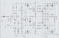
This is a schematic of my latest amp. It is a quasi-complimentary design running mosfet outputs.
The prototype running on my bench with the rails noted delivers around 200 watts into 8 ohms. The amp is very quiet and seems to be very low in distortion (I have trouble measuring below 0.1%).
With the right power supply and FETS it could deliver maybe around 800 watts or more into 2 ohms. The protype is running IXYS26N50 FETS and 4 or 5 of these per rail would be up to it.
The one planned for my Hi-Fi will run IRFP450's. These seem to be more linear and approach clipping better.
Want more power - add more FETS (and power supply)
Anyway feedback and ideas are welcome.
Cheers
Attachments
quasi: Hi, and congratulations on your design!
There are a number of things that you should probably take a closer look at:
The MJE350 needs to build up about 14 Volts on the 100 Ohms in the bottom, this gives you 140 mA @ 70 Volts drop before the IRFP's kick in. 140 mA @ 70V is 10 Watts, i think well over the max limit of the MJE350.
Also to run the BC550's in the input stage with a 70 V collector potential, is a bit over the safe limit.
There are also a few other thing i would do differently, but then, we are all different")
All the best from
Lars
There are a number of things that you should probably take a closer look at:
The MJE350 needs to build up about 14 Volts on the 100 Ohms in the bottom, this gives you 140 mA @ 70 Volts drop before the IRFP's kick in. 140 mA @ 70V is 10 Watts, i think well over the max limit of the MJE350.
Also to run the BC550's in the input stage with a 70 V collector potential, is a bit over the safe limit.
There are also a few other thing i would do differently, but then, we are all different
All the best from
Lars
Hey thanks Lars;
In the prototype the input and driver stages are running the same rails as the output stage.
In my next amp the rails will be seperated as shown in the circuit. This is probably why I haven't blown up the MJE350, so your feedback has already been valuable. In the current setup it only develops about 4 volts @ 40 milliamps on the 100 ohm.
But with the rails tied the +ve rail FET clips before the -ve rail and this is my main reason for going to the higher driver stage rails.
I wonder if I can leave the negative rail tied and just lift the positive rail for the driver stage?
The BC550 is a mistake from a previous drawing. The input stage runs BC546's.
Thanks again & cheers
Hi quasi !
I think even for the bc546 70v is a bit much, maybe you should
cascode them ? (The same for Q1)
The feedback-resistor (33k) should be same size as inputres (22k),
this reduces dc-offset and might eliminate the need for VR1, and
replace it with good metal-resistors.
You might consider adding basestoppers (~1k) to q1/q5, i had once
the experience that this kind of circuit can flip at startup, providing
full supplyvoltage at output. This can happen if the amp clips to
negative side, driving q5 into reverse bias. In this case q5 "sucks"
out all current via it's base from the 2diodes, shutting down q1,
keeping the amp in it's clipped state. This is some horrorscenario, but
possible. This destroyed one of my testspeakers. Only switching off
the amp pulls it out of this state again... (or q5 burns up)
To be really sure, use two separate ccs.
Mike
Your driver stage is very different then i have seen. Most have a resistor tied between the 2 driver transistor and the gate drive is taken from either side of that resistor and its associated drive transistor.
I have never seen a drive system where the gate drive is taken from a V drop across a resistor to the speaker line and V- system before.
Zero
I have never seen a drive system where the gate drive is taken from a V drop across a resistor to the speaker line and V- system before.
Zero
Hi Quasi
The upper FET Vgs accurately tracks the voltage drop across Re of q7. OK here, all quite conventional.
But the lower arm FET Vgs is trying to track the voltage across Re of q7 plus the voltage difference between driver stage -Vrail and current stage -Vrail. Any slight variation between these two voltages will modulate the current through the output FETs and thus the output voltage.
I believe the quasi output driver voltage must accurately follow any droop under load of the hi current rail. Unless the designer adopts a special circuit to accurately track the -Vrail voltage then the driver MUST run on a common -Vrail with the current output.
Comments from the knowledgeable most welcome.
regards Andrew T.
Thanks MikeB;
I have never experienced the fault you have described but I do see your point. I always have DC detect on the output of my amps and this saves the speakers. Yes I would probably lose bits of the amp. Seperate voltage references for these current sources is quite easy.
Thanks Zero Cool;
Transistor Q8 and it's collector resistor provides the bias voltage for the negative rail output stage. It is similar to a quais-complimentary bi-polar output drive but instead of driving the base of the output stage directly it provides a voltage ref. for the output FET.
Thanks AndrewT;
You are of course correct. The prototype on my bench has both the positive rails and negative rails tied together at +/- 60v and the reference for the output FETS is the same on both sides.
I want to seperate the rails and run a fully regulated supply for the input and driver stages at a higher voltage for two reasons.
1. I hope to achieve less ripple on the input and driver stages.
2. I want to be able to drive the FET on the positive rail fully and avoid it clipping some 5 volts before the negative rail FET does.
Note I haven't done this yet and indeed advice from Lars has probably saved at least 1 MJE350 and who knows what else.
I think I have 2 maybe 3 options;
1. Leave it as it's running now on common rails, forget about the assymetric clipping and be happy.
2. Change Q8's collector resistor to 350 ohms to provide 14v across it. I.e. 4v+(70v-60v). But then this stage would be assymetric.
3. Leave the negative rail tied to the 60v rail and provide regulated +70v to the other side only. This seems ok but I'm worried that I have missed a consequence of this.
Thanks all for your input.
Quasi
Thanks MikeB again (forgot this bit);
Yes, the BC546's are probably just hanging on with around 58 volts across them (currently 60 volt rails). So yes a cascode will be used. Under this arrangement I'll drop around 50 volts across cascode BC546's and leave 10-20 volts across BC550's (they're quieter) for the diff. pair.
The voltage across Q1 is about 45 volts and is currently a BC546. This should be ok.
Your advice about the feedback resistor and input resistor is noted and I'll probably change the input resistor. I still want the amp to have a gain of around 33. I'll probably leave VR1 there so I can get near enough to 0.00v offset.
All of the fixed resistors in the amp are metal film (except for the output stage).
Thanks again for your valuable feedback.
Cheers
Quasi
Commentable thoughts
Hello Quasi I have seen ur Circuit which has following Mistakes in Practical world.
Input Transistors VCE limit is outreached.
The Voltage accross them are more than there specified limit instead of it use 2N5551/2N5401 Trannies.
The lower side Driver stage resistor is not tied to lower side mosfet source. A fatal mistake for destruction of ur mosfets.
No use of emmiter resistor with lower side driver.
You have to tie the driver stage with VCC's of mosfets and only the Voltage amplification stage is to be tied seperatly at +-70VDC.
Take a look at these mistakes, Hope u eradicte these problems
Workhorse Technologies.
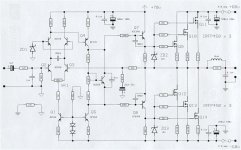
Revised circuit
Thanks for your feedback and constructive criticism.
I have made the following changes for the next prototype.
1. Cascode first stage leaving about 20 volts across the diff . pair.
2. Resistor feeding the diff pair upped from 10k to 15k to take some voltage away from Q1.
3. Only one negative rail tying the driver stages to the output FETS.
4. Leaving the higher positive rail to drive the positive output FETS fully and removing the assymetric clipping problem.
5. 12v zeners on the FET gates to provide some protection against overdrive (during excessive currnt draw).
6. Shifting the current sharing resistors to the negative rail FETS source.
7. Input resistor changed from 22k to 33k to match feedback resistor.
The new cct is attached. How does it look now?
Attachments
Hi quasi !
2 things:
1, For ZD1 use a ~22k or 47k resistor to positive voltage,
2, Paralell to the 33k at input 1nF seems too much to me, try 330pF
I still think you should get rid off VR1, with matched resistors
feedback/input and the 22uf-cap (maybe use 100uF?) DC should
be very low. If not, something else is wrong.
Don't forget, when VR1 is not in middle, the diffamp gets asymetrical,
producing strange distortions.
Mike

Thanks MikeB;
Ok, Ok, Ok. I'll tell you what. I'll use VR1 during the setup phase. Then I'll measure what it's set at and replace it with e metal film resistor network This will be quite easy using PCB stand-offs.
The zener? Doh! Doh! Doh! I just forgot to draw it. I was going to use 22k.
Yeah I'm happy with 330pf.
I would have thought that 22uf in the feedback loop would be enough...oh well a 100uf would fit and I can't see a down side.
Thanks Circlotron;
Hi Quasi,
Add caps to shunt out noise on zd1, try electrolytic//small film.
zd2 & zd3 must come after the gate resistors. Otherwise there is no limit on zd current, then its a fight between mj340 and zd2 to see who survives longer!!! You need a zd across EACH gate to source, not across gate to rs. Check your current through the fets for a 12v Vgs and also check power across the fet in current limit condition. I think 12v might need to be reduced.
Should the feedback time constant (22u*1ko=22ms) be bigger or smaller than input time constant(4u7*33k=150ms)? Someone else suggested NFB cap @ 100uF maybe even bigger?
regards Andrew T.
Thanks AndrewT;
Youre suggestion about the bypass caps for the cascode zener is noted.
Dunno what I was thinking with these zeners. Put them in there without too much thought. I think I'll have to do without them otherwise my gate resistors will have to be too high to limit the current through the zener (if they ever turned on).
Yeah looks like the 100uf feedback capacitor is a goer.
Thanks & Cheers
Hello quasi,
do not omit the Fet gs zeners. They are the standard method of protecting the Fets.
1. they prevent you exceeding the maximum gate voltage.
2. they give a very simple current limit circuit for both overdrive and short circuit conditions.
design your pcb with provision for fitting them, you could them decide for fit or not. ps. the gate zeners are your last resort to stop the FETs dying.
regards Andrew T.
Hi Quasi,
Few questions/comments
1) What is the purpose of the 100pF in the input stage between the collectors of Q2 and Q3? That's the cascode mid-point -- very low impedance.
2) 100n pot in the input. Should this not be replaced by fixed Metal film resistors. The large DC NFB should take care of any output DC offsets.
3) Again not sure about the 100pF between the base and emitter of Q7, Q8. I don't see anything in the circuit to ensure stability -- R - C pole zero network placed between the 1K resistors on the collectors of the cascode, or Miller RC between the collector of Q4 and its base.
Dinesh
Those zeners
Thanks AndrewT;
Yes those zeners will provide a degree of overcurrent protection and around 8 volt ones will do it. Trouble is as the cct stands they will blow up either themselves or/and the mje350/mje340 transistors if they turn on.
I could put individual ones on each FET gate but with the gate resistors at only 22 ohms there will be around 2 amps flowing through the zeners. I know this will be momentary but it still is brutish.
I would need to raise the gate resistors to over 100 ohms each (still too low really) but this increases the drive impedance. So I just don't know.
Another way of protecting against over current is to monitor the current through the source resistors on the FETS. A transistor switch here could shut down the driver stage or indeed the whole amp.
I'll ponder all this tonight and hopefully post my decision soon. Any ideas (from anybody) are welcome.
Cheers
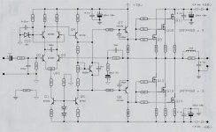
Schematic update
This is where I'm at.
Changes made from last schematic are;
1. The BC550's are back in a cascode arrangement with about 35 volts across each one.
2. The constant current source is a BC550 as well with about 30 volts across it.
3. Basic filtering has been applied to ZD1.
4. The gate zeners on the output FETS have been removed. Higher value gate resistors will be tried during testing and if appropriate zeners may be re-introduced and connected directly to each FET gate.
5. The feedback capacitor has been increased to 100uf plus a 33pf capacitor has been added across the 33k resistor.
6. The input bypass capacitor has been reduced to 330pf.
Thanks for everyones input. This amp schematic reflects a lot of the ideas presented.
Now I gotta design and make the new board. Maybe some photos to come later. If anyone is interested I can post a photo of the original prototype.
Thanks again and Cheers
Attachments
- Home
- Amplifiers
- Solid State
- Power amp under development