To SPLIF or not to SPLIF ... that is the question
quasi,
I just happened to come across 'The ALTMANN "SPLIF" Amplifier Topology"
<http://www.altmann.haan.de/splif_page/>
again while searching for something elese on internet.
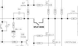
The actual execution of this seems farily simple for your amp design I sense. I am not sure as I am not an "expert". If I understand the implementation of SPLIF and your amp design the SPLIF occurs in the area of Q7, Q8, Q9 and Q12 as per the attached schematic section I have edited to show (to save complicated and excessive words") )
)
If you try it while remaining aware of points related to bias and offset as the information explains it woudl be interesting to know if you feel ther eis some value to this SPLIF idea. Seems in theory to make sense.
Regards,
John L. Males
Willowdale, Ontario
Canada
15 December 2004 23:48
quasi,
I just happened to come across 'The ALTMANN "SPLIF" Amplifier Topology"
<http://www.altmann.haan.de/splif_page/>
again while searching for something elese on internet.
The actual execution of this seems farily simple for your amp design I sense. I am not sure as I am not an "expert". If I understand the implementation of SPLIF and your amp design the SPLIF occurs in the area of Q7, Q8, Q9 and Q12 as per the attached schematic section I have edited to show (to save complicated and excessive words
)If you try it while remaining aware of points related to bias and offset as the information explains it woudl be interesting to know if you feel ther eis some value to this SPLIF idea. Seems in theory to make sense.
Regards,
John L. Males
Willowdale, Ontario
Canada
15 December 2004 23:48
Attachments
Re SPLIF;
It's a coincidence. This is something that I tried just two days ago. This forces that stage to self centre rather than reference to the output.
I am going to re-visit this option after I finish the amp.
There are other possibilities here also e.g. the swith could be replaced with a resistor and another to ground to provide localised feedback for that stage. This is something else that I plan to try.
But I have spent enough time trying different things, it is now time to finish.
Thanks for taking the time to communicate your findings.
Cheers
Re[03]: Re SPLIF
Hi quasi,
When you tried this what listening and/or measuring differences did you expereince in general? In other words does this help or a case of 6 of one half dozen of other?
Regards,
John L. Males
Willowdale, Ontario
Canada
16 December 2004 00:07
quasi said:It's a coincidence. This is something that I tried just two days ago. This forces that stage to self centre rather than reference to the output.
Cheers
Hi quasi,
When you tried this what listening and/or measuring differences did you expereince in general? In other words does this help or a case of 6 of one half dozen of other?
Regards,
John L. Males
Willowdale, Ontario
Canada
16 December 2004 00:07
Re: Re[03]: Re SPLIF
I realised after I posted my response that what I tried was in fact different to what you posted. In my setup the 33k feedback resistor was still tied to the output i.e across the SPLIF. In my setup Q7 & Q8 connected directly to each other without connecting to the output. This forces them to find their own centre reference. When I tested this I only did so via the CRO whilst connected to a 4 ohm load. It seemed fine i.e good waveform at 10Khz. That is the only testing I did beacuse of the reason I gave about finishing above.
To amp_man_1
Yes, this endeavour to get more peak to peak swing out of this amp is starting to tell me I shoudn't bother. It seems that I should pull the negative swing short rather than try to increase the positive swing, and a resistor on Q8 helps to do that.
What I have decided to do is to finish this amp with common rails throughout and play again another day working through the learnings I have made (with the help of this forum).
I am quite happy with it's performance with common rails in any case.
Cheers
keypunch said:
Hi quasi,
When you tried this what listening and/or measuring differences did you expereince in general? In other words does this help or a case of 6 of one half dozen of other?
Regards,
John L. Males
Willowdale, Ontario
Canada
16 December 2004 00:07
I realised after I posted my response that what I tried was in fact different to what you posted. In my setup the 33k feedback resistor was still tied to the output i.e across the SPLIF. In my setup Q7 & Q8 connected directly to each other without connecting to the output. This forces them to find their own centre reference. When I tested this I only did so via the CRO whilst connected to a 4 ohm load. It seemed fine i.e good waveform at 10Khz. That is the only testing I did beacuse of the reason I gave about finishing above.
To amp_man_1
Yes, this endeavour to get more peak to peak swing out of this amp is starting to tell me I shoudn't bother. It seems that I should pull the negative swing short rather than try to increase the positive swing, and a resistor on Q8 helps to do that.
What I have decided to do is to finish this amp with common rails throughout and play again another day working through the learnings I have made (with the help of this forum).
I am quite happy with it's performance with common rails in any case.
Cheers
Re: To SPLIF or not to SPLIF ... that is the question
I think, there is wrong slpit place is shown. First mosfet pair MUST be in
feedback loop. Splitting must be done between the first and the rest mosfet
pairs.
Just my mind.
Do not splif anything before your or my version will be proved by
gurus
Andrew
keypunch said:quasi,
I just happened to come across 'The ALTMANN "SPLIF" Amplifier Topology"
<http://www.altmann.haan.de/splif_page/>
again while searching for something elese on internet.
The actual execution of this seems farily simple for your amp design I sense. I am not sure as I am not an "expert". If I understand the implementation of SPLIF and your amp design the SPLIF occurs in the area of Q7, Q8, Q9 and Q12 as per the attached schematic section I have edited to show (to save complicated and excessive words
If you try it while remaining aware of points related to bias and offset as the information explains it woudl be interesting to know if you feel ther eis some value to this SPLIF idea. Seems in theory to make sense.
Regards,
John L. Males
Willowdale, Ontario
Canada
15 December 2004 23:48
I think, there is wrong slpit place is shown. First mosfet pair MUST be in
feedback loop. Splitting must be done between the first and the rest mosfet
pairs.
Just my mind.
Do not splif anything before your or my version will be proved by
gurus
Andrew
Re[05]: To SPLIF or not to SPLIF ... that is the question
Hi Andrew,
My appologies, youare absolutely correct my Post #121
<http://www.diyaudio.com/forums/showthread.php?postid=534292#post534292>
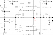
schematic segment to show the SPLIF location was incorectly placed. My appologies gents. I have posted with this message the corrected SPLIF.
In adding a SPLIF the way I have done to the existing amp design of quasi will need add another output driver pair to restore the intended power design handling of the amp. I did not add an extra output device pair to this schematic example of quasi's amp design as I do not have the software or design file.
Regards,
John L. Males
Willowdale, Ontario
Canada
16 December 2004 02:18
anli said:
I think, there is wrong slpit place is shown. First mosfet pair MUST be in
feedback loop. Splitting must be done between the first and the rest mosfet
pairs.
Just my mind.
Do not splif anything before your or my version will be proved by
gurus
Andrew
Hi Andrew,
My appologies, youare absolutely correct my Post #121
<http://www.diyaudio.com/forums/showthread.php?postid=534292#post534292>
schematic segment to show the SPLIF location was incorectly placed. My appologies gents. I have posted with this message the corrected SPLIF.
In adding a SPLIF the way I have done to the existing amp design of quasi will need add another output driver pair to restore the intended power design handling of the amp. I did not add an extra output device pair to this schematic example of quasi's amp design as I do not have the software or design file.
Regards,
John L. Males
Willowdale, Ontario
Canada
16 December 2004 02:18
Attachments
Re: Re[04]: The long and wordy
The reason you often see an amp put out e.g. 100/120/140 for 8/4/2 is that the power supply is not actually up to the task of delivering the 140 watts and is collapsing. A good supply should allow the amp to double it's power output each time the load impedance is halved. There may be a slight discrepancy as when you increase the load you get more losses in the output stage, however it should be approaching a doubling.
keypunch said:Interesting answer re 30/60/120 for 8/4/2. There are man using other designs suggesting can use very safely at much higher wattage ratings. This not to disagree with your suggestion and confirm of my questions. This is exacly why I ask questions and then with the information I make a collective decision.
The reason you often see an amp put out e.g. 100/120/140 for 8/4/2 is that the power supply is not actually up to the task of delivering the 140 watts and is collapsing. A good supply should allow the amp to double it's power output each time the load impedance is halved. There may be a slight discrepancy as when you increase the load you get more losses in the output stage, however it should be approaching a doubling.
quasi,
I forgot to mention it last time, but it came back to me during a random moment of thought If you make the emitter resistor of Q8 the same value as that on the collector it runs the Sziklai pair at unity gain and will better balance out both the turn on characteristics and swing with the upper half of the output stage
I forgot to mention it last time, but it came back to me during a random moment of thought
If you make the emitter resistor of Q8 the same value as that on the collector it runs the Sziklai pair at unity gain and will better balance out both the turn on characteristics and swing with the upper half of the output stage Hi!
The post are way to long to read, and i don't have the knowledge concerning solid state to make anything out either way, but i wonder what progress you'v made with the amp Quasi?
i'm really wanting to make myself a good bass amp to complement the gc when bi-amping
regards
marius
The post are way to long to read, and i don't have the knowledge concerning solid state to make anything out either way, but i wonder what progress you'v made with the amp Quasi?
i'm really wanting to make myself a good bass amp to complement the gc when bi-amping
regards
marius
Hey richie00boy;
Yes I have tried this this stage with a 100ohm resistor on Q8's emitter and it will be included in this build.
Hey demogorgon;
The amp research and development is finished. Tomorrow I am building the second board and power supply. I am going to run +/- 72 rails to achieve just over 200 watts into 8 ohms and about 350 watts into 4. The design is about 90% of what I wanted but it is time to finish and build it.
It could make a great bass section amp.
Cheers
splif
Hello All,
about a year ago, I build the splif topology as added in the word file.
My opinion about it:
First I build an amplifier with just one pair of BJT's driving the speaker, however the damping was very low and so the bass tones were not "tight"". So I build another with 10 parallel pairs in the output. Attached the schematic.
I listened to it for about half a year, and didnot like the sound anymore, the amplifier simply is not linear, and this is audible.
instruments like a saxophone sound good, but the rest of the instruments simply do not sound natural.
I want to state that this is my personal opinion, maybe someone else thinks different about this.
Best Regards:
Nexus
Attachments
Final Schematic;
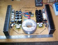
This is the final schematic of the amp module. Two modules have been built and it is time to assemble the complete amp.
The major changes to the design are;
1. The split supplies have been removed and common rails feed the whole amp.
2. The cascode transistors have been removed from the input stage and replaced with a current mirror (Q4 & Q5). This change has been made to ensure symetrical current flows through Q2 & Q3.
3. Removing the cascode stage has required high voltage transistors for Q2 & Q3. I have settled on 2SC1845. These are low noise transistors with Vce of 120 volts.
4. Some resistor and capacitor values have been changed to try and achieve a balance of noise, distortion and thermal peformance.
There are other improvements that can be made to this schematic and these will be implemented at another time. But this is the schematic that will be put to service in the completed amplifier.
Many forum contributors will see their suggestions in this schematic and to you I say thankyou.
Cheers
Attachments


Thanks hienrich, demogorgon & rajeev;
Thanks heaps for your compliments. This has taken a long time but it's getting closer to the end.
When it is finished I will post all the ccts and layouts for anyone who is interested.
During this exercise I have found areas that can be improved but the board layouts don't allow this easily. Even so the amp as it is performs very well, is very quiet and clean.
I will attempt some specifications when the case is finished and all the components are fixed.
The best part about this amp is that it has been built using mostly second hand parts found in junked electronics (power supplies etc.) or parts recycled from other projects. To date the whole project has cost under $100 AUS ($75US) and I have everything I need for the case.
Thanks once again for your kind thoughts.
Cheers & Happy New Year
- Home
- Amplifiers
- Solid State
- Power amp under development