Sorry dinesh didn't see your post.
The 100pf capacitor between the diff pair serves to shunt any high frequency that may be here and amplified through the stages. This may not be a problem all the time but I have fixed troublesome amps this way before. I first got this idea from an Elektor cct I saw years ago. They used a resistor+cap but I found that a small capacitor worked much the same.
The 100 ohm trimpot serves to adjust the output offset caused by tolerance issues in the input stage. The feedback will only drive the offset down so far and I like to get it as close to 0.00 as I can. Once the setting is determined it can be replaced with a resistor network to suit.
The small capacitors on Q7 and Q8 shunt any RF away from their bases. Yes I am paranoid about the FETS oscillating. Your views about Q4 make sense. I'll just use a small capacitor though and omit the resistor.
Thanks for your feedback
Cheers
Umm ...I haven't explained the motivation behind a quasi-complimentary amp.
Thers is one compelling reason; I have literally a bucketful of new and used N channel MOSFETS including IRFP450, IRFP250, IXFH26N50, IRF820 (TO220), philips BUK series and assorted others. Thought I might as well use them.
Cheers
Thers is one compelling reason; I have literally a bucketful of new and used N channel MOSFETS including IRFP450, IRFP250, IXFH26N50, IRF820 (TO220), philips BUK series and assorted others. Thought I might as well use them.
Cheers
Hi quasi !
The point is, that the 100pf is on the wrong side of the cascode,
it needs to be above. But a RC is better, like 330pf+330ohm or
something like that. You might use a 1n+330ohm, then make
cdoms smaller. Your feedback-cap (33pf) might be too big, think
more about 15pf.
Mike
The point is, that the 100pf is on the wrong side of the cascode,
it needs to be above. But a RC is better, like 330pf+330ohm or
something like that. You might use a 1n+330ohm, then make
cdoms smaller. Your feedback-cap (33pf) might be too big, think
more about 15pf.
Mike
Each capacitor you place shunting the signal path to ground [or as a miller capacitor] with no resistor in series causes an additional pole to be introduced in the open loop response. If it's a RC network then it causes a pole-zero
Each transistor adds also a pole or a pole-zero to the open loop response. Each pole produces additional phase lag so phase margin is reduced. I wouldn't add extra poles to the circuit if I was you
In the other hand, those RC networks you've seen are not intended to reduce RF pickup, they are part of the compensation strategy to reduce gain at high frequencies to a suitable value and make the circuit stable [and this pole-zero compensation strategy was common in Elektor circuits]
Okay, mystical to the sound... I was surprised by the improvement
to the sound. As i found out with my last amp, phasecompensating
is extremely important, with simple changes this amp changed from
unpleasant sounding to extreme good sounding.
What i didn't get, is there a formula for the ratio R <-> C ?
My method for adjusting is not very scientific, i find these values
by trying with acsweep in sims...
Mike
Thanks Eva and MikeB
Aaaaaah .....thanks.
Eva are you saying that all by capacitors on the base-emmitter junctions should have a resistor? None of the amps I have seen do this, maybe beacuse there is always a resistor feeding the base anyway.
I forgot to shift it when I inserted the cascode. Ok the resistor is in.
those RC networks you've seen are not intended to reduce RF pickup, they are part of the compensation strategy to reduce gain at high frequencies to a suitable value and make the circuit stable
Aaaaaah .....thanks.
Each capacitor you place shunting the signal path to ground [or as a miller capacitor] with no resistor in series causes an additional pole to be introduced in the open loop response. If it's a RC network then it causes a pole-zero
Eva are you saying that all by capacitors on the base-emmitter junctions should have a resistor? None of the amps I have seen do this, maybe beacuse there is always a resistor feeding the base anyway.
The point is, that the 100pf is on the wrong side of the cascode,
I forgot to shift it when I inserted the cascode. Ok the resistor is in.
Quasi,
Loose the caps across the emitters of the cacode. The input impedance at those nodes is ~26 ohms (since it appears you are running 1mA per leg of the diff pair). Any pole introduced by the cap is way up in frequency. There are two reasons for the caps -- as Eva and the rest have mentioned -- the first for compensation. In which case the cap goes across the 1K ohm load resitors on the input diff pair. You *donot* wan't to put a cap alone -- a series RC is better. Why ? Because, with a large step applied at the input (yes I know that the input RC would prevent this) the amp will slew. Slewing is bad because the output is not related to the input.
The other place small caps are placed is across the input of the diff-pair, to avoid RF getting into the inputs and being recrtified by the base-emitter of the inputs (you get to hear AM broadcast radio from the AMP when this happens). This is rarely required in discrete designs (often needed in BJT op-amp designs) because the current levels in the input stage is fairly high (you are at 1mA). This keeps Vbe at fairly large levels and prevents RF rectification.
There is no needed to place these caps across the B-E junctions of the emitter followers Q7 and Q8.
I know I am repeating this.... If you want to keep the pot to zero the offset you make want to place resistors lets say 100ohms from emitter to the wiper point. This is to prevent the unforseen. Lets say the wiper opens for a short instant of time (pots are crummy). Q4 base goes high . Q4 tuns off. Power amp output becomes stuck at the negative rail, loud pop from speaker ....
Lets say you did have an offset and you moved the pot. Notice that you are changing the emitter degeneration resistor. This means that you are changing the open loop gain. Right now you probably have 1mA in the leg (Re = 26/Ie ~ 26ohm). Your gain for the first stage alone is 1000/(50+26) on this stage with pot at center ~ 13 (hope you are not superstitious). With wiper at other extreme it would be 1000/(100+26) ~8, and at the other 1000/26 ~40. If you do wan't to do a zero offset you may be better off injecting a small voltage into the negative input (create a small variable +ve, -ve voltage from supplies and feed it to the top of the 100uF/25V cap).
--
Dinesh
Ok....
Everybody happier now?
Seriously thanks for all your input. Many suggestions have been implemented in the design.
Yes I'm sticking with the output offset control, but I have made it fail safe. I.e. if the wiper goes open cct, nothing (practically) happens.
Cheers
Everybody happier now?
Seriously thanks for all your input. Many suggestions have been implemented in the design.
Yes I'm sticking with the output offset control, but I have made it fail safe. I.e. if the wiper goes open cct, nothing (practically) happens.
Cheers
Attachments
Hey Circlotron;
Yea.....I only intended to post this picture maybe 2-3 times, but with all the advice....oh well the amp looks better day by day.
I only have a dos based schematic drawer (sad but true). I could download a better one, but I would have to learn it and time is an issue.
This means I gotta print it, scan it, reduce it, adjust it before I post it. A real pain in the neck.
Cheers
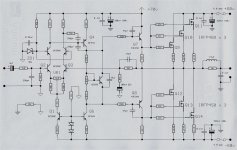
amp under development
Hi quasi,
It is a great fun to design one's own. Looking at your design I would try the following changes:
1. Generally, driver transistors (here Q7 and Q8) are run from unregulated supplies together with power devices (Q9 to Q14). See Silicon Chip Ultra Low distortion amplifier: issues November 2001 to January 2002. These show how it is usually done together with board layouts for the amps and power supplies. All the other transistors should be on the regulated, symetrical PS. However, there are exceptions and Stochino runs his driver transitors from the regulated supply - see Alex Soton site for details. You may have slight problem as your output is not complementary so some gymnastics might be needed. Anyway the regulated supply should be symetrical and include Q1,Q5 emiter sides to get the full benefits of regulation.
2. 220uF on board filtering for the output stage is not enough. You need at least 1,000uF (Stochino uses 3x470uF per rail and 470uF per regulated rail). My suggestion would be to use fast audiograde NICHICON Muse KZ caps 330uF/100V from Handmade. These are U$ 1.30 each while here downunder you have to pay that much for lousy grade commercial caps. These caps are to care for transients so no point to use anything less than NICHICON KZ or FG, ELNA Cerafine or alike.
3. It has been demonstrated (see Douglas Self, Holton) that distortions are reduced if the NFB loop starts just before the output filter and goes 'forward', rather than 'backward', to NFB gain setting resistors (the cap across the 33k could possibly be reduced to 10pF-22pf as already suggested by other forum members). Usually it's best to use solid coper link and design layout in such a way that the linked distance between the NFB origin, the gain resistors and Q3 input are as short as possible. On top of it 'Star' ground design boards have their merits (see Silicon Chip) and remember that board layout must well handle high output currents.
4. Do not use ceramic caps in audio amps. They may even sing when excited to their resonance frequency. Use high quality high voltage silvered (muscovite) mica. The only place where good quality ceramics could be used are power supplies - as snubing caps on rectifiers (bridges) to be precise.
5. The input differential pair ideally should be factory matched. If you would like to improve on BC550c use 2sc2240bl (2sa970bl is its complement) Toshiba transistors (Lobtron has these). These are very low noise, high grade audio transistors especially designed for input stages. These trans, however, have different lead configuration, namely: E,C,B.
6. Try to replace MJEs and possibly BFs with 2sb649A / 2sd669A. You can get them from the Company store. These are very good drivers used extensively by Randy Sloane and others. You may opt for the C series (hfe: 100-200). At worst use new Motorola devices as in Ultra Low Distortion amp - see SC.
7. Input HF cut of filter according to Duncan should be about -3dB between 250-300kHz. The input cap (4.7uF) should be metalised polypropylene fast speaker grade one (eg Solen).
8. more importantly, the NFB cap should be of highest possible quality. NICHICON ES bipolar 220uF/50V would be among the best contenders. It should be paralleled by 1uF (or somewhat less) fast metalised polypropylene. NICHICON is available from Handmade for just over U$1. But if you manage to reduce DC on the output to acceptable levels without a cap in the NFB then go for it but without factory matched input pair it would be difficult.
9. the 14uH inductor looks huge to me. With well designed amp it should not be higher than 2-3uH (In fact, a well designed amp should function well without it but some inductance does not do any harm). Soild coper (or silver if you like it), at least 1.5-1.8mm, wire should be used with that many Watts you want to pump into your speakers.
10. For power supply designs see Alex Soton and read Dejan from TNT. "Double" bridging in unregulated supplies has a few merits and does not cost much.
11. To minimise the impact of filtering caps on the power supply rails solder 1ohm/10W non-inductive resistor with 680nF/160V+ metalised polypropylene between the unregulated power supply input points on boards and dirty ground. Prof. Otala invented that and it works (see Otala's amp or TNT).
12. You will also need fast filtering caps and at lest 25mF (25,000uF) per rail. The best bargins here are ELNA LPO (audio grde) caps 8.2mF/71V (8200uF) sold by Solen Canada. They cost less than **** grade caps you get in Australia and are twice as fast. Much more expensive alternatives involve Sikorel and NICHICON FG and Super Through (Percy Audio sells them).
13. If you well match Vgs of your IRFs then you may try to reduce their resistor values down to 0.33ohm if possible. Duglas Self demonstrates that output stage linearity is degraded as resistor values INCREASE. Similarly the choice of gate resistors is important.
14. Finally, if amp is running well you may try to reduce Miller caps from 100pF down to 47pF as in the Stochino amp but probably not below that value. It will somewhat improve the slew rate.
Well, I think I have covered most of the issues and hope that I did not messed up too much with your design.
Be glad to hear your comments when the amp is finished and runs!!!
Cheers,
Janusz
Commentable thoughts
Hi OLD FRiend CIRCLOTRON I Think Ur AVATAAR Reflects ur Possesion of Knowledge Regarding Image Processing That why its Quality is High Enough .
With Regards,
WORKHORSE TECHNOLOGIES")
Circlotron said:Hey quasi, you can get the pic to be a lot sharper (and a lot smaller file size)if you post it as a gif or png with the contrast cranked right up.JPG is only good for photo type pics, not line drawings. GIF/PNG is also excellent for screen captures.
Hi OLD FRiend CIRCLOTRON I Think Ur AVATAAR Reflects ur Possesion of Knowledge Regarding Image Processing That why its Quality is High Enough .
With Regards,
WORKHORSE TECHNOLOGIES
Thanks janusz;
Thanks for spending the time you did checking out my schematic.
My thoughts as follows;
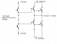
1. Yes the best result would be for regulated supplies to the driver stages, but while this is easy for a complimentary output stage it isn't for a quasi-complimentary design. Please see my reasons for a quasi-comp design posted earlier. In this design the pre-output stage of Q8 must be tied to the same rail as Q12-Q14 because of the reference created across the 100 ohm resistor. On the positive side I have upped the driver rail to +70v. This is mainly done to drive Q9-Q11 fully, i.e provide sufficient gate/source voltage. If I don't then this side will clip some 5 volts before the negative rail FETS. I could regulated the positive driver stage rail only I suppose. Hmm....
2. Yep, noted.
3. Yes the board layout is important. I've no doubt that when (if) I post it there will probably be more feedback than I have received already. You will notice in the schematic both quiet and noisy grounds. The quiet ground is fed by a 10 ohm resistor. Every grounded component will return via an exclusive track to this ground. Same is true for the "power" ground.
4. Noted. All my powersupply capacitors are bypassed using ceramics. Capacitors in/near the signal path are poly. This amp will use components already in my possesion. No reason an esoteric version couldn't be made using expensive parts.
5. I had over a thousand BC550C's (picked em up for around $0.03 Aus each) of which I have used sold, donated, destroyed about half. Man I even use them in my DC detect circuit so I'm gonna use them in the amp. Again an esoteric version ...etc.
6. Refer response 5. Similar situation.
7. Noted. I have some polyester (I think) capacitors ranging up to 4u7. I was gonna use these. The cct shows an electrolytic...this is a remnant of a previous design.
8. Noted.
9. Noted. In practice this value is not critical as it will not affect anything in the audio range. However the lower this inductance the more current through the output capacitor. My compromise is 14 uH. I don't subsribe to silver windings (or silver anything (Jewellery excluded) let alone silver speaker cables...damn I promised myself not to go there... The coil will be fat.
10. Yep I read that and I'll use it (even if I may not hear the difference). Similar situation to response 5 (how many do you need?) I also have a hundred or so mega fast TO220 style rectifiers ....I wonder..... hmm....naahh.
11. Umm....okay.
12. Similar situation to response 5. I have lots of big fat (new and secondhand) capacitors. I was going to run around 50,000uf.
13. I was toying with the idea of no drain resistors and using matched FETS.....but later on I want to provide overcurrent protection by monitoring the current through these. 0.33 v 0.47 hardly worth it really...but I'll see whats in the bucket.
14. Miller caps are 47pf in the third stage. Yep 47pf for second stage is cool.
There is a prototype of this amp already running. I does not have the cascode input stage or the 70v rail for the early stages. It runs BC546's and the driver transistors as shown. There are other differences which have been corrected via this forum.
That "primitive" prototype has been well received by local critics (boozy mates). I'll post regularly on the progress of Version 2 (or is that v1.2 or v1.1.....damn you software houses).
Thanks for your interest and feedback.
Cheers
Thanks for spending the time you did checking out my schematic.
My thoughts as follows;
1. Yes the best result would be for regulated supplies to the driver stages, but while this is easy for a complimentary output stage it isn't for a quasi-complimentary design. Please see my reasons for a quasi-comp design posted earlier. In this design the pre-output stage of Q8 must be tied to the same rail as Q12-Q14 because of the reference created across the 100 ohm resistor. On the positive side I have upped the driver rail to +70v. This is mainly done to drive Q9-Q11 fully, i.e provide sufficient gate/source voltage. If I don't then this side will clip some 5 volts before the negative rail FETS. I could regulated the positive driver stage rail only I suppose. Hmm....
2. Yep, noted.
3. Yes the board layout is important. I've no doubt that when (if) I post it there will probably be more feedback than I have received already. You will notice in the schematic both quiet and noisy grounds. The quiet ground is fed by a 10 ohm resistor. Every grounded component will return via an exclusive track to this ground. Same is true for the "power" ground.
4. Noted. All my powersupply capacitors are bypassed using ceramics. Capacitors in/near the signal path are poly. This amp will use components already in my possesion. No reason an esoteric version couldn't be made using expensive parts.
5. I had over a thousand BC550C's (picked em up for around $0.03 Aus each) of which I have used sold, donated, destroyed about half. Man I even use them in my DC detect circuit so I'm gonna use them in the amp. Again an esoteric version ...etc.
6. Refer response 5. Similar situation.
7. Noted. I have some polyester (I think) capacitors ranging up to 4u7. I was gonna use these. The cct shows an electrolytic...this is a remnant of a previous design.
8. Noted.
9. Noted. In practice this value is not critical as it will not affect anything in the audio range. However the lower this inductance the more current through the output capacitor. My compromise is 14 uH. I don't subsribe to silver windings (or silver anything (Jewellery excluded) let alone silver speaker cables...damn I promised myself not to go there... The coil will be fat.
10. Yep I read that and I'll use it (even if I may not hear the difference). Similar situation to response 5 (how many do you need?) I also have a hundred or so mega fast TO220 style rectifiers ....I wonder..... hmm....naahh.
11. Umm....okay.
12. Similar situation to response 5. I have lots of big fat (new and secondhand) capacitors. I was going to run around 50,000uf.
13. I was toying with the idea of no drain resistors and using matched FETS.....but later on I want to provide overcurrent protection by monitoring the current through these. 0.33 v 0.47 hardly worth it really...but I'll see whats in the bucket.
14. Miller caps are 47pf in the third stage. Yep 47pf for second stage is cool.
There is a prototype of this amp already running. I does not have the cascode input stage or the 70v rail for the early stages. It runs BC546's and the driver transistors as shown. There are other differences which have been corrected via this forum.
That "primitive" prototype has been well received by local critics (boozy mates). I'll post regularly on the progress of Version 2 (or is that v1.2 or v1.1.....damn you software houses).
Thanks for your interest and feedback.
Cheers
Commentable thoughts
Shouldn't the transistor (Q7 in my cct) providing the bias for the positive rail FET have it's collector tied to the +70 volt rail? Otherwise it cannot deliver enough gate voltage with respect to the FET's source to turn it on fully.
In my design I thought about splitting the rail between the collector resistor of Q8 and the emitter resistor of Q5 the using a -70 volt rail for the first and second stage. But in practice it would not make any difference (that I could see) except make the circuit look more symetrical.
Please tell me if my thinking is weird.
Cheers
Re: Commentable thoughts
Hi QUAZI
You Dont Have to Tie the Collector of Driver transistor which biases the upperFet Because A voltage swing of Higher magnitute is already available from The voltage amplification Stage to drive this stage.
Secondly A Misconception Regarding Full ON i.e. Full Saturation Of Mosfet.
In Linear CLASS-AB AMP The Output Voltage Swing Must Remain in Linear domain of Mosfet within Applied Specific VCC , So as to Avoid Saturation which Introduces Distortion. Secondly In this type Of implementation The pre-Clipping is Avoided and post Clipping is driving the Mosfet to semi-Saturation condition Only.
As the RDS of Mosfets is minimum generally when the Gate to Source Voltage reaches about 10 to 12VDC which can only be realised through switching circuits not in our case in which it is Linear, the gate voltage seldom reaches 8 to 9 Volts only in peak conditions.
Secondly One has to create a symmetric driver stage in order to sustain equal driver excitation during high Temp rise conditions.
THirdly In a Music Sequence such as percussion or Piano waves there are very asymmetric in nature therefore care must be taken to ensure proper current draw from the driver stage which Clearly effects the Negative and positive Slew rates or rise time of waves to ensure integrity and avoid smearing of bass instruments.
With Regards
WORKHORSE TECHNOLOGIES
quasi said:Shouldn't the transistor (Q7 in my cct) providing the bias for the positive rail FET have it's collector tied to the +70 volt rail? Otherwise it cannot deliver enough gate voltage with respect to the FET's source to turn it on fully.
In my design I thought about splitting the rail between the collector resistor of Q8 and the emitter resistor of Q5 the using a -70 volt rail for the first and second stage. But in practice it would not make any difference (that I could see) except make the circuit look more symetrical.
Please tell me if my thinking is weird.
Cheers
Hi QUAZI
You Dont Have to Tie the Collector of Driver transistor which biases the upperFet Because A voltage swing of Higher magnitute is already available from The voltage amplification Stage to drive this stage.
Secondly A Misconception Regarding Full ON i.e. Full Saturation Of Mosfet.
In Linear CLASS-AB AMP The Output Voltage Swing Must Remain in Linear domain of Mosfet within Applied Specific VCC , So as to Avoid Saturation which Introduces Distortion. Secondly In this type Of implementation The pre-Clipping is Avoided and post Clipping is driving the Mosfet to semi-Saturation condition Only.
As the RDS of Mosfets is minimum generally when the Gate to Source Voltage reaches about 10 to 12VDC which can only be realised through switching circuits not in our case in which it is Linear, the gate voltage seldom reaches 8 to 9 Volts only in peak conditions.
Secondly One has to create a symmetric driver stage in order to sustain equal driver excitation during high Temp rise conditions.
THirdly In a Music Sequence such as percussion or Piano waves there are very asymmetric in nature therefore care must be taken to ensure proper current draw from the driver stage which Clearly effects the Negative and positive Slew rates or rise time of waves to ensure integrity and avoid smearing of bass instruments.
With Regards
WORKHORSE TECHNOLOGIES
- Home
- Amplifiers
- Solid State
- Power amp under development