Hello,
Well, the hum went down after running the ransformer for a few seconds. After I out a piece of rubber under the torroid it went away.
Concrete:
Primary-wirering was correct.
secondary wasn't connected at all, actually I emediately checked if the scondaries are shorted-they weren't.
Remains the possibility of a shorted turn, or bad mains-voltage. The torroid was custom made by a small german company- they should have a good quality control. I still have the results of measurements they made (isolation-voltage and loadregulation).
Last thing I did was to leave the torroid on the mains, since the hum was very small. All secondary voltages were perfectly OK.
Greetings
Black
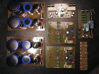
PS: These are the finished Boards for my NMOS. Tomorrow I'll start mounting the Fets and the MJEs on the heatsink") Cant wait to test these Modules with my Lab-PSU
Cant wait to test these Modules with my Lab-PSU
Hi,
a big hum could be mis-wired primary, or shorted secondary, or shorted turn, or DC from the mains, or poor quality control from the factory.
Well, the hum went down after running the ransformer for a few seconds. After I out a piece of rubber under the torroid it went away.
Concrete:
Primary-wirering was correct.
secondary wasn't connected at all, actually I emediately checked if the scondaries are shorted-they weren't.
Remains the possibility of a shorted turn, or bad mains-voltage. The torroid was custom made by a small german company- they should have a good quality control. I still have the results of measurements they made (isolation-voltage and loadregulation).
Last thing I did was to leave the torroid on the mains, since the hum was very small. All secondary voltages were perfectly OK.
Greetings
Black
PS: These are the finished Boards for my NMOS. Tomorrow I'll start mounting the Fets and the MJEs on the heatsink
Cant wait to test these Modules with my Lab-PSUAttachments
BlacK_Chicken said:Hello,
PS: These are the finished Boards for my NMOS. Tomorrow I'll start mounting the Fets and the MJEs on the heatsink
Hi Black,
Nice work.
I am curious about your PSU. It looks like you have 3 different sizes of filter capacitors. One pair, the Black looking ones (no pun on your name intended) look th smallest. Did you design your PSU with 3 different size filter capacitors on purpose? If so your reason(s)? I know there is a school of though about to use different rather than the same size in the PSU, but I have yet to understand the reason(s).
Regards,
John L. Males
Willowdale, Ontario
Canada
16 February 2007 10:22
P.S. I have not had the time in almost a week to continue the forum research on the specs of the quasi amp. I had some unexpected matters arise. jlm
PSU....
Hello Keypunch,
In short:
No.
There was some development. At first I had 4 of these smaller 4-pin Philips "LL" caps (4700µ) left over from my Symasym. With these I wanted to form one commen PSU for both channels. Then I got the Possibility to get these Philips 5-pin "LL" caps (10 000µ). I ordered 8 of these - intended for a split PSU. But I only got 4 of them - they were out of stock. After that i went for the small ones on ebay, more for psychological than for electrical reasons. I personally dont think that 3300µ more per rail make such a differnce.
Update: Today I completed one channel. Half an hour ago I wnated to test it on my bench. But on applying +-30V my Lab-PSU was shorted, the current-regulation went into action for a limited current of 100mA.
No further measurement were done, I wanted to heave a break.
I check things this eavening.
Greetings
Black
Re: it works!
Congratulations. You'll have to post some photos. I am interested to find out how quiet the amp is in terms of residual noise. Well done again
Cheers
Quasi
BlacK_Chicken said:Hello again,
It works perfectly....
It was a bit of solder between the TO220 pads..
Plays musik nice.
DC-offset ca. 1,5mA.
Bias 60mA
Greetings
Black
Congratulations. You'll have to post some photos. I am interested to find out how quiet the amp is in terms of residual noise. Well done again
Cheers
Quasi
Residual noise....
Hello Quasi,
I dont exactly understand "residual noise"in this context. If you want to know if the NMOS200 is noisy (noise from the AMP, no RF, no music, no hum - am I right?), I dont think it is.
On the bench with all those flying leads, bad PSU (high ripple), bad grounding and no rf-shielding (because there is no metal case) AMPs are imo always noisier than the finished amp.
Today my NMOS was a bit noisy at first. I had connected the input-GND to the main-GND, not the the floating input-GND (only for testing purpose, I now I am lazy ). After input-GND was connected there was less noise. On top my testing speaker is very "noisy" (hard to explain, one reason might be the high efficency - probably up to 100dB/1 meter).
I think that this AMP is going to be dead-quiet, once its finished.
Regards,
Black
Hello Quasi,
Congratulations. You'll have to post some photos. I am interested to find out how quiet the amp is in terms of residual noise. Well done again
I dont exactly understand "residual noise"in this context. If you want to know if the NMOS200 is noisy (noise from the AMP, no RF, no music, no hum - am I right?), I dont think it is.
On the bench with all those flying leads, bad PSU (high ripple), bad grounding and no rf-shielding (because there is no metal case) AMPs are imo always noisier than the finished amp.
Today my NMOS was a bit noisy at first. I had connected the input-GND to the main-GND, not the the floating input-GND (only for testing purpose, I now I am lazy
). After input-GND was connected there was less noise. On top my testing speaker is very "noisy" (hard to explain, one reason might be the high efficency - probably up to 100dB/1 meter).I think that this AMP is going to be dead-quiet, once its finished.
Regards,
Black
Update....
Hello again,
My second channel is working now. No problems so far.
->Bias 60mA
->DC-Offset 0,8mV (!)
These figures are measured with very high quality DMMs, with high accurancy.
Supply voltage again was +-32V (I dont get more out of my Lab-PSU), The currents in the diffenrent stages match well to given currents.
One thing that might be interesting:
The bias current is not shared equally between the Mosfets , if I measure the voltaes across the paraleled 1R resistors (source-resistors) i get very different current ratings. They range from 10mA to 40mA.
But its playing music very nice.
Shamefully I have to travel to work next tuesday, therefore have to wait some weeks until I come back to finish my NMOS.
Many thanks to Quasi for publishing (and develloping) this wonderful Project!
Regars,
Black
Hello again,
My second channel is working now. No problems so far.
->Bias 60mA
->DC-Offset 0,8mV (!)
These figures are measured with very high quality DMMs, with high accurancy.
Supply voltage again was +-32V (I dont get more out of my Lab-PSU), The currents in the diffenrent stages match well to given currents.
One thing that might be interesting:
The bias current is not shared equally between the Mosfets
, if I measure the voltaes across the paraleled 1R resistors (source-resistors) i get very different current ratings. They range from 10mA to 40mA. But its playing music very nice
.Shamefully I have to travel to work next tuesday, therefore have to wait some weeks until I come back to finish my NMOS.
Many thanks to Quasi for publishing (and develloping) this wonderful Project!
Regars,
Black
Hi,
how many pairs are you using?
How close did you match them?
What current did you select for matching?
Did you match the emitter resistor values?
Any one of those could cause at least part of your problem.
But first, insert a shorting plug in the input and disconnect all output loads then do the tests again.
An alternative to the shorting plug is a plug fitted with a ground to input resistor that matches the source resistance (Rs) of the source component (preamp)
Hi,
All measurements were done without any load and with the iunput shorted to ground. When I know everything is ok then I connect a speaker - just to have some fun, not for serious testing.
Fets werent matched at all. The only transistors I matched were the 2sc1845 at the input. The Source resistors werent matched too, but I dont think that is a problem because these are 1R/5% in paralel.
Iam running 2 Pairs of IRF640N.
I dont actually know If this really IS a problem, maybe the current sharing is better when the amp is working under normal conditions.
If I remeber correctly the current range was between 12 and 37mA on my last channel. I havent measured the singele current on the first one.
Greetings
Black
Hi,
it is a problem, but you have to decide if it causes a serious enough temperature worry to make you change it.
You have 8 devices in your two channels. You can match them into 4 pairs. You can then put them together in an amp with no further worries.
Now, each of the high current (low Vgs) Fets is carrying 3 to 4 times as much current as it's high Vgs partner. This makes the FET Tc run hotter than it's partner. It may also increase the sink temperature locally around the hot device (the amount of local temperature rise depends on sink thickness).
If you stress the hot device, it is more likely to fail than the cooler device. i.e. it runs closer to it's SOAR limit. Decision time.
The resistor tolerance is MUCH closer than the errors you have measured, so they are giving a close enough indication, but if you decide to do some Vgs matching at Ib then consider doing some resistor matching as well.
Hello,
Yeah, you are right. Of course.
Well, before it was a brief measurement, I will have to redo these measurements on both channels properly. After that I decide wht to do.
On the one hand I use the more powerful 640N (instead of Quasis 840) and my Bracket has 4mm thickness. On the other hand I want the best performance possible from my amp.
Is it possible to use the voltages across the source-resistors for the matching? It would be definately easier to change one or two fets in between channels than desmounting all fets and remount them after matching.
Thank You.
PS
How are all other NMOS Amps behaving? Do they all hacve equal currents?
Hi,
it will be a bit of a gamble but you could pick the worst FET and swap it for the partner of the other worst FET.
Do not compare upper pair to lower pair.
Compare the bias between each side of a parallel pair.
This would be
fet1a=low bias=high Vgs
fet1b=high bias =low Vgs
fet2a=high bias =low Vgs
fet2b=low bias =high Vgs
so swapping 1a with 2a puts two high Vgs together and two low Vgs together.
Worth the experimant to see if they are a little better or much better or swapped around the other way.
You can meassure the Vgs in circuit but each are passing a different current so this may be worthless, but a pattern may emerge that helps select new partners.
Well done again Black. Good luck with matching the FETs although don't get too hung up about it. Get them closer if you can and then measure under signal conditions (CRO is best). I think you'll find they'll share better then.
Anyway I see you are using 2SC1845's for the input pair. What voltage rails do you intend using?
Cheers
Q
Anyway I see you are using 2SC1845's for the input pair. What voltage rails do you intend using?
Cheers
Q
Hi Quasi,
but that still allows the low Vgs partners to run hotter than the remainder. That pulls the SOAR nearer the "under signal condition" and still puts the hotter devices at higher risk of failure....under signal conditions (CRO is best). I think you'll find they'll share better then.
Thanks...
Hello Andrew and Quasi,
first, 2sc1845:
I am going to use a 2x35VAC transformer, the rails will probably range from 45-50VDC. I just used the Japanese types because I personally think they have better quality than the common BC types. Nothing special. I had 6 pieces of 2sc1845, while matching I noticed that they all were extremly similar - matching was more ore less obsolete.
second, matching:
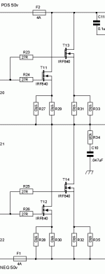
I have atteched a part of the shematic for my NMOS (the To-220 version).
If I understand correctly (that is what I would do), I have to compare the pairs - as the same current should be running throuh both of them.
The first pair would be T11&T12(A) the second pair would be T13&T14(A) - (A) and (B) for the different channels.
Now I would compare T11&T12(A) with T11&T12(B), if there are huge differences in current I swap two fets to combine these with higher Vgs and these with lower Vgs. Am I right???? Same for T13&T14 (A) and (B).
BTW: What is "CRO", testing under (and with) constant sinus wave into an resitive load isn't it?
Regards,
Black
Hello Andrew and Quasi,
first, 2sc1845:
I am going to use a 2x35VAC transformer, the rails will probably range from 45-50VDC. I just used the Japanese types because I personally think they have better quality than the common BC types. Nothing special. I had 6 pieces of 2sc1845, while matching I noticed that they all were extremly similar - matching was more ore less obsolete.
second, matching:
I have atteched a part of the shematic for my NMOS (the To-220 version).
If I understand correctly (that is what I would do), I have to compare the pairs - as the same current should be running throuh both of them.
The first pair would be T11&T12(A) the second pair would be T13&T14(A) - (A) and (B) for the different channels.
Now I would compare T11&T12(A) with T11&T12(B), if there are huge differences in current I swap two fets to combine these with higher Vgs and these with lower Vgs. Am I right???? Same for T13&T14 (A) and (B).
BTW: What is "CRO", testing under (and with) constant sinus wave into an resitive load isn't it?
Regards,
Black
Attachments
Hi Black,
It's the parallel pair 11&13 that need matching then 12&14 to match.
no.The first pair would be T11&T12(A)
It's the parallel pair 11&13 that need matching then 12&14 to match.
Hello,
Thank you Andrew.
Now, this is what I measured right now. Bias was set to 60mA in total.
Channel A:
T11 - VR=0,8mV, VGS=2,87V
T13 - VR=15,4mV, Vgs 2,86V
T12 - VR=8,6mV, VGS=3,18V
T14 - VR=7,5mV, VGS=3,18V
Cannel B:
T11 - VR=17,7mV, VGS=2,935V
T13 - VR=0,25mV, VGS=2,957V
T12 - VR=11,85mV, VGS=2,975V
T14 - VR=6,68mV, VGS=2,99VV
Well, I think I leave it as it is, the VGS voltages are quite similar.
Any suggestions?
Thanks alot.
Black
Hi Black,
I see that if you add Vgs to Vre you almost get a match across the FET + source resistor. These two voltages should be identical, have a look at the schematic and you'll see why.
I also see that channel A T12&14 are almost equal (only +14%).
Channel B T12&14 are badly in need of re-arranging (+77%).
The other two pair are a disaster, with over 95% of Iq passing through one FET. That's what happens with Vfets and their wide spread of parameters.
I recommend you remove these 6FETS and group them into pairs.
You should aim for Vgs difference <20mV at the same current for each pair, if you can't get close to 20mV just do as best you can with the FETs you have.
Work at low voltage to minimise the heat dissipation causing Tj to rise excessively. Even doing this you will have to try and take the measurements at the same time increment into the test so that each junction is near the same temperature. 10seconds and 8V may get you close enough.
BTW,
Iq=60mA is low for FETs, that's just 30mA each.
Most recommend over 50mA and some say over 100mA.
Borbely says over 100mA each AND about 500mA total.
I have some laterals set at 75mA each and only the the heatsinks prevent me going higher (4pair @ 69Vdc = 41W).
- Home
- Amplifiers
- Solid State
- Power amp under development