Pejinm,
Your layout configuration is very different. I have never seen a configuration where the fins are turned facing in. As you are very good with number comments/questions I will again pose in that manner:
1) Why did you decide to face the fins inside the case?
2) I have to assume the reason for the fan is largely a result of the heatsink fins facing inside?
3) For the heat disapaited from the input pre-driver/driver stage how will that heat be disapaited so it does not build up around the driver stage components? From what I can observe of your pics with case it seems the board areas will be in a mostly isolated internal air space. Correct?
4) Have you found a way to secure the one output driver that you had some challenges securing with a screw yet? I ask as I am assuming that if that one output driver is not physically secured like the others it may be more prone to the device die heat build up, which might lead to its failure.
Regards,
John L. Males
Willowdale, Ontario
Canada
07 May 2006 13:39
Hi John,
1) I faced the fins inside because I wanted to have some shielding between transformer and modules (less interferance), and it was the only way to mount these sort of heatsink securly and with less drilling of the case.
2) yes.
3) I will see how it's heating once I turn up the amp, but I belive that it has a good pasive cooling.
4) yes.
Regards,
Miodrag Pejin
Nice Job Ahmad
It looks like you're going to bring the leads up through the holes and solder to pins on the PCB were the FET legs would normally go. Is that right?
If so twist the leads a little and keep them as short as possible.
Good luck with the rest of the project.
Cheers
It looks like you're going to bring the leads up through the holes and solder to pins on the PCB were the FET legs would normally go. Is that right?
If so twist the leads a little and keep them as short as possible.
Good luck with the rest of the project.
Cheers
Miodrag,
Thanks for your reply.
1) Interesting reason. As I mentioned I not seen anyone do make effort to isolate a toroid before. I guess most feel the level of transformer field raidiation was low compared to distance from toroid to modules. It makes sense for sure. Personally I like to keep as much as possible passive thermal cooling. I appaud your well thought out approach and rational to your approach.
1b) I had been thinking of making the amp PSU external. The reason was driven more from a flexibility and physical standpoint. The toroids in question are 6 inches (15cm) in diameter, and about 5 inches (12.5 cm) high, not to mention the weight about 12 pounds (27kg). As you can see, the weight and dimension of these 1127 VA or 926 VA toroids is large. Also one can run at least 3, in practice 4, modules. A case for 4 modules, toroid, and PSU for each module which has seperate rectifiers for + and - side of the rails is real formula to massive and very heavy final execution in the usual manner. Ergo seperate case for each module, toroid in own case and PSU's each in own case is the likely approach for these large toroids. I have some more "civil" size toroids and I will likely do like most diy and commerical units which is how quasi did for his first completed unit.
3) I will be interested in your assessment of the pre-driver/driver heatsink under moderate to above moderate drive levels for extend periods of time. Say Organ music?? If you prefer a test signal is ok too. Passive here is good") I sure hope the passive cooling works for the heatsink
I sure hope the passive cooling works for the heatsink
4) I am very happy you were able to secure that one output driver.
You are doing a very fine job with the project with your solid thinking and reasoning for how and why you make the decisions that are important to your DIY version of your amplifier.
I suspect others following this project will look forward to hearing how you find the completed project and your opinions of the design variants you choose.
Regards,
John L. Males
Willowdale, Ontario
Canada
08 May 2006 05:12
Thanks for your reply.
1) Interesting reason. As I mentioned I not seen anyone do make effort to isolate a toroid before. I guess most feel the level of transformer field raidiation was low compared to distance from toroid to modules. It makes sense for sure. Personally I like to keep as much as possible passive thermal cooling. I appaud your well thought out approach and rational to your approach.
1b) I had been thinking of making the amp PSU external. The reason was driven more from a flexibility and physical standpoint. The toroids in question are 6 inches (15cm) in diameter, and about 5 inches (12.5 cm) high, not to mention the weight about 12 pounds (27kg). As you can see, the weight and dimension of these 1127 VA or 926 VA toroids is large. Also one can run at least 3, in practice 4, modules. A case for 4 modules, toroid, and PSU for each module which has seperate rectifiers for + and - side of the rails is real formula to massive and very heavy final execution in the usual manner. Ergo seperate case for each module, toroid in own case and PSU's each in own case is the likely approach for these large toroids. I have some more "civil" size toroids and I will likely do like most diy and commerical units which is how quasi did for his first completed unit.
3) I will be interested in your assessment of the pre-driver/driver heatsink under moderate to above moderate drive levels for extend periods of time. Say Organ music?? If you prefer a test signal is ok too. Passive here is good
I sure hope the passive cooling works for the heatsink 4) I am very happy you were able to secure that one output driver.
You are doing a very fine job with the project with your solid thinking and reasoning for how and why you make the decisions that are important to your DIY version of your amplifier.
I suspect others following this project will look forward to hearing how you find the completed project and your opinions of the design variants you choose.
Regards,
John L. Males
Willowdale, Ontario
Canada
08 May 2006 05:12
Hi Ahmad,
A few quick questions if I may:
1) It looks like the board is mounted on the standoffs on the heatsink. If this is true, can you briefly explain why you choose to use wires from output drivers to PCB?
2) Are the wire lengths as you have made them in the second posting pic with output drivers mounted?
3) Are your output drivers insulated with something like a mica, silcon pad under? I see the silcon grease. I ask as some people on diyAudio say no insulating pad is needed if one is careful when mounting to an andozied heatsink. Ergo why I asked this question.
4) I cannot see in either of your pics how you will do the T8 - Vbe. I cannot see a Vbe on the heatsink. How are you going to ensure you have a Vbe to correct device?
I will be interested in your thoughts of using short twisted wiring brom board to output device. One of my mounting options is via wires from PCB to devices on heatsink. The other mounting option would be output devices at right angles to PCB and a mount devices on the common and mounting elements. I am leaning to latter approach.
Keep up your excellent work Ahmad.
Regards,
John L. Males
Willowdale, Ontario
Canada
08 May 2006 05:32
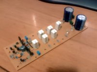
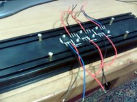
hi all , and thanks for comments ,
sure i ll keep wires as short as it can thnx .
to John :
1) at first i wanted to mount the FETs under the board and on the heatsink as common , but the grooves on heatsink didn t lemme that , so i had no way but mount FETs on heatsink and connect them to pcb with short wires ,and then mount the pcb on heatsink w 4 standoffs , as u see .
2) yeah the wires are bout 5 inches , as u see i already soldered them to FETs , and ready to solder to main pcb , as quasi guessed i m going to bring up the leads through the holes and solder from the upside of PCB . i hope i got ur question right
3) yeah the FETs are not connected to together , cuz of the black color layer on whole heatsink . but i used silicon grease .
4) bout T8 , as i said the whole project is not completed yet , i leave bout .25 inch space between 2nd and 3rd FETs to mount the T8 there , i ll make a hole for T8 there and will mount it w silicon grease and a pice of aluminium as u can see in the pic i attached .and finally will connect it to pcb w short wires ( hope i got ur question right and answered to it , i m not sure i got it right lol )
thanks again
,yeah quasi that s exactly wat i m going to do ,It looks like you're going to bring the leads up through the holes and solder to pins on the PCB were the FET legs would normally go. Is that right?
sure i ll keep wires as short as it can
thnx .to John :
1) at first i wanted to mount the FETs under the board and on the heatsink as common , but the grooves on heatsink didn t lemme that , so i had no way but mount FETs on heatsink and connect them to pcb with short wires ,and then mount the pcb on heatsink w 4 standoffs , as u see .
2) yeah the wires are bout 5 inches , as u see i already soldered them to FETs , and ready to solder to main pcb , as quasi guessed i m going to bring up the leads through the holes and solder from the upside of PCB . i hope i got ur question right
3) yeah the FETs are not connected to together , cuz of the black color layer on whole heatsink . but i used silicon grease .
4) bout T8 , as i said the whole project is not completed yet , i leave bout .25 inch space between 2nd and 3rd FETs to mount the T8 there , i ll make a hole for T8 there and will mount it w silicon grease and a pice of aluminium as u can see in the pic i attached .and finally will connect it to pcb w short wires ( hope i got ur question right and answered to it , i m not sure i got it right lol
)thanks again
Attachments
Hi Ahmad,
I've also read the view of using the anodised layer as insulation, but it is too risky in my view. The anodised layer is very thin and heating and cooling stresses plus the odd knock or vibration could cause it to break down over time. I might be over cautious but I would use insulating pads.
In the end it's up to you, just make sure that you measure an open cct from the heatsink to the FETs drain.
Cheers
Hi Ahmad,
Thanks for your reply. Yes you answered the questions just fine.
3) I have been thinking for lower thermal resistance I might consider a direct mount using the anodized layer as the "insulating" element. You, as I have been for some time, should give serious consideration to quasi's comments with respect to this. I am trying to come up with a "creative" solution that best deal with the issues or finds a "balance" between the concerns quasi raised. This is in part why I am interested in the sonic and stability of the amp by using wires to the module for the output drivers. Part of my creative solution may mean I have to run wires to the output drivers from the module.
lol lol lol Why did I know quasi would suggest mounting in such a manner (with no mica or silcone pad, et al) "... is too risky in my view.", "I might be over cautious but I would use insulating pads." Not to worry quasi, you raise very valid concerns in such a direct mount of output drivers. quasi makes a good point to remind you "just make sure that you measure an open cct from the heatsink to the FETs drain."
4) Excellent how you have thought not only to leave the extra space between the output devices, but that you wish to place the T8 Vbe between a pair of output devices. One of the changes I have not done to the modified PCB's I have posted a while back is to open up some extra spacing between a pair of output devices on same rail if someone wants to do as you have. For me I need a bit more space between. I want to use a TO-126 case type for the Vbe to be mounted between a pair of output devices on same rail. I am also trying to come up with a few other "creative" Vbe mounting/thermal solutions. These will likley require increasing the spacing of at least those output driver devices involved.
As this is the first time I have built a solid state amp I been learning alot and researching as much as I can on some key areas. I have lots of experience working with high voltage laser printers so I am very aware of the voltages that may be involved. I have built a tube amp some time ago. I want to avoid a suitation where I need to re-work in major manner the module and heatsinking elements and also ensure my first crack at the PSU is well thought out. The idea is to avoid alot of "tinkering" after fact. Some tinkering may be needed being a DIY project, but I like to use the best practices of others experience as I have a desire to build a set of amps and then be done for most part. I have a few add-ons I want to do like VU meter, balanced inputs, some creative PSU handling of module power up sequencing, thermal cut off switch, clipping indicator, etc. Some of those may need to be done after the basic amps are built. I have a list so I can ensure a case can handle these items. I really like quasi's design for its stability and ability to be a flexible in transistor choices and still provide a excellent amp. For this I am very greatful for quasi's efforts in his design and rounding in during the design opinions of others to come to the current design he has. Sadly I have not had the time I like and need to organize the many excellent postings iabout this design and many have asked so it is easy to find and hopefully reduces some of the more common questions asked on the thread. I sure hope to soon, even if I do so in stages.
Regards,
John L. Males
Willowdale, Ontario
Canada
08 May 2006 13:23
08 May 2006 13:32 As "usual", typo corrections.
Thanks for your reply. Yes you answered the questions just fine.
3) I have been thinking for lower thermal resistance I might consider a direct mount using the anodized layer as the "insulating" element. You, as I have been for some time, should give serious consideration to quasi's comments with respect to this. I am trying to come up with a "creative" solution that best deal with the issues or finds a "balance" between the concerns quasi raised. This is in part why I am interested in the sonic and stability of the amp by using wires to the module for the output drivers. Part of my creative solution may mean I have to run wires to the output drivers from the module.
lol lol lol Why did I know quasi would suggest mounting in such a manner (with no mica or silcone pad, et al) "... is too risky in my view.", "I might be over cautious but I would use insulating pads." Not to worry quasi, you raise very valid concerns in such a direct mount of output drivers. quasi makes a good point to remind you "just make sure that you measure an open cct from the heatsink to the FETs drain."4) Excellent how you have thought not only to leave the extra space between the output devices, but that you wish to place the T8 Vbe between a pair of output devices. One of the changes I have not done to the modified PCB's I have posted a while back is to open up some extra spacing between a pair of output devices on same rail if someone wants to do as you have. For me I need a bit more space between. I want to use a TO-126 case type for the Vbe to be mounted between a pair of output devices on same rail. I am also trying to come up with a few other "creative" Vbe mounting/thermal solutions. These will likley require increasing the spacing of at least those output driver devices involved.
As this is the first time I have built a solid state amp I been learning alot and researching as much as I can on some key areas. I have lots of experience working with high voltage laser printers so I am very aware of the voltages that may be involved. I have built a tube amp some time ago. I want to avoid a suitation where I need to re-work in major manner the module and heatsinking elements and also ensure my first crack at the PSU is well thought out. The idea is to avoid alot of "tinkering" after fact. Some tinkering may be needed being a DIY project, but I like to use the best practices of others experience as I have a desire to build a set of amps and then be done for most part. I have a few add-ons I want to do like VU meter, balanced inputs, some creative PSU handling of module power up sequencing, thermal cut off switch, clipping indicator, etc. Some of those may need to be done after the basic amps are built. I have a list so I can ensure a case can handle these items. I really like quasi's design for its stability and ability to be a flexible in transistor choices and still provide a excellent amp. For this I am very greatful for quasi's efforts in his design and rounding in during the design opinions of others to come to the current design he has. Sadly I have not had the time I like and need to organize the many excellent postings iabout this design and many have asked so it is easy to find and hopefully reduces some of the more common questions asked on the thread. I sure hope to soon, even if I do so in stages.
Regards,
John L. Males
Willowdale, Ontario
Canada
08 May 2006 13:23
08 May 2006 13:32 As "usual", typo corrections.
Hi all , and thank u so much for suggestions and replies , ur comments keep me warm to go on
thanks ...
sure i ll use mica ( or silicon pad if i can find some )I've also read the view of using the anodised layer as insulation, but it is too risky in my view.
thanks ...
This is a bit OT, but I had a question about the DC protection circuitry. Having read Rod Elliot's project 33 on the same thing, it is said that using a simple diode across the relay will slow its response too much:

My question is, would it be advantageous to modify the protection circuitry to something similar to what Rod has come up with?The relay(s) must be turned off in the shortest possible time, so the use of the normal protection diode across the coil should not be used, as it slows the response considerably. Instead, the arrangement shown still protects the driver transistor, but allows the relay magnetic field to collapse without generating a current in the coil (this the what slows the relay's release).
Hi,
even though I have never noticed a previous reference to the diode slowing the release time of the relay, I have no reason to doubts ESP's findings.
I would go along with his suggestion.
Why do so many recommend the diode solution without pointing out the pitfall, only conveniently mentioning the advantage.
Is that the modern way? Always sell the idea and to heck with the consequences!
Hi PM650,
I doubt the other scheme shown will affect the release time of the relay much.
It's true that as long as current is flowing in the coil, there will be magnetism generated to hold the pole in. The voltage build up would be so fast that the alternate arrangement shown may not really change anything in a meaningful way.
In short, I doubt very strongly that the other circuit will improve things, and if it did, not in a worthwhile amount. So the single reverse biased diode does it's job well (protecting the transistor switch).
-Chris
The other point Andrew, is that the voltage would almost instantly climb to a point that would cause the other diodes to conduct. You would still have current flow as before. Failing that, the transistor may fail (short of course) making the protection circuit a non-issue.
Remember we are talking about current flow through an inductor. It's going to conduct somewhere. Quickly.
In any event, I doubt the timing is significant. Remember there is a delay in detection as well depending on the magnitude of the offset.
-Chris
Remember we are talking about current flow through an inductor. It's going to conduct somewhere. Quickly.
In any event, I doubt the timing is significant. Remember there is a delay in detection as well depending on the magnitude of the offset.
-Chris
quasi,
Quicki questions for you regarding C7, the 100uF feedback capacitor to ground:
1) Is it bi-polar or electrolytic?
2) For the PSU size you built for your pair of amps what is the minimum, and most comfortable working voltage rating you would use?
3) I seem to have a problem finding the physical size, let alone the 100uF value (which should not really be hard to find at all), that will fit on the PCB. Is it better to go up to 150uF/220uF or down to 68uF/47uF? From my research most designs use a 100uF value or back to back 100uFs to behave like a bi-polar. Hence the question of 47uF, as I recall serious caps of same value equation simplifiers to 0.5 x c.
Regards,
John L. Males
Willowdale, Ontario
Canada
12 May 2006 13:21
Hi Keypunch,
the NFB lower leg DC blocking cap should be as good quality you can afford. To achieve the necessary time constant the RC value needs to be about 14times the value for your high pass roll off frequency (bass lower limit). To get there you need a very large resistor in the lower leg (bad for noise) or a high capacitance.
This forces you to adopt electrolytics although some use tantalum caps.
If you want good phase response down to 20Hz your low frequency roll off needs to be about 2Hz. The NFB RC then needs to be about 100mS. 1k0 + 100uF achieves this.
The calculation for series caps is the same as for parallel resistors i.e. C1*C2/(C1+C2), so your example of C+C=C/2 is correct. Then 1k0+220uF+220uF gives near enough the same answer. When series connecting electrolytics some recommend adding a bias voltage to the C junction point to ensure the electrolytics never feel a reverse voltage and keeps the chemical film established.
- Home
- Amplifiers
- Solid State
- Power amp under development