The schematic of this preamp is here
I made this PCB but I don't like it Dimensions is 155*45 mm and the pots are not on board so there will be many wires
How could it be better??
The PCB was made in P-CAD 2001 so if someone wants .pcb file let me know (.bmp file is bad because I don't know how to export the image from P-CAD so I just did the screenshot)!
PCB is in attachment in a zip file.
I made this PCB but I don't like it
Dimensions is 155*45 mm and the pots are not on board so there will be many wires How could it be better??
The PCB was made in P-CAD 2001 so if someone wants .pcb file let me know (.bmp file is bad because I don't know how to export the image from P-CAD so I just did the screenshot)!
PCB is in attachment in a zip file.
Attachments
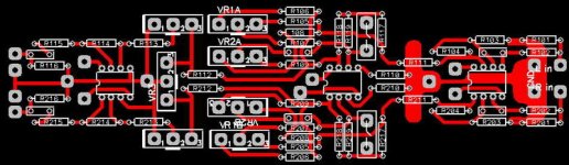
Thanx destroyer, only problem is that there will be many (MANY) wires on it
It is preamp.
Link: http://sound.westhost.com/project97.htm
It is preamp.
Link: http://sound.westhost.com/project97.htm
a couple of quick comments
Layout looks pretty good. Nice and symmetrical.
A few comments...
On U1 it is good to keep the track area extending from the inverting input as small as possible. You can make this better by swapping the connections on R104 and R204.
I assume the power and ground connections are just left of U1 on the pcb. I see no decoupling on the pcb nor in the schematic. Op-amps should always have local decoupling.
The gound points for the volume/balance circuit (U3) do not appear to connect to the ground point left of U1. How will you ensure correct ground referencing?
Again, try to reduce the track area off the inverting inputs of U3.
I'd increase the dc bleed resistors R101, R201, R116, R216 to 1Mohm. No point in unecessarily loading circuits.
I pressume C103 and C203 are non-polarized.
Having lots of wires to the pots isn't necessarily a problem. Just keep the wires as short as you can and closely bound to reduce loop areas. Computer ribbon cable is good for this.
Good luck...hope it sounds good.
Re: a couple of quick comments
1. Yes, I know what you mean...I'll fix that
2. I was thinking to connect the grounding with another wire or on PCB all free space to use as ground. I'll send it back here when I update the board.
3. Yes, C103 and 03 are non-polarized - would it be better if they are?
Thanx for comments! I hope it will too!
traderbam said:
On U1 it is good to keep the track area extending from the inverting input as small as possible. You can make this better by swapping the connections on R104 and R204.
The gound points for the volume/balance circuit (U3) do not appear to connect to the ground point left of U1. How will you ensure correct ground referencing?
Again, try to reduce the track area off the inverting inputs of U3.
I pressume C103 and C203 are non-polarized.
Good luck...hope it sounds good.
1. Yes, I know what you mean...I'll fix that
2. I was thinking to connect the grounding with another wire or on PCB all free space to use as ground. I'll send it back here when I update the board.
3. Yes, C103 and 03 are non-polarized - would it be better if they are?
Thanx for comments! I hope it will too!
Upopa's got a very good point. You should definitely put some bypass capacitors on the board too.
And why not try to make a layout, that resembles the one on the picture http://sound.westhost.com/p97.jpg ?
IMHO you should keep the potentiometers on the board as well. Nothing but trouble will come out of it, if you do not.
And why not try to make a layout, that resembles the one on the picture http://sound.westhost.com/p97.jpg ?
IMHO you should keep the potentiometers on the board as well. Nothing but trouble will come out of it, if you do not.
Mlaen said:So, where should I put them
I tried to keep the pots on board but then I can't make the PCB
Can't make the PCB? Why is this?
You mentioned 155*45 mm. Is that the max. size or what? Is it a board size problem or a enclosure problem?
I would like the board to be as smallest as possible
I'm beginner in PCB design (if you could call this PCB design) so it's too hard for me to make the PCB with pots on board (+they are stereo)
Thanx for that, I'll fix that over the weekend, now I don't have the time
I'm beginner in PCB design (if you could call this PCB design) so it's too hard for me to make the PCB with pots on board (+they are stereo)
Running the R- and L-channel signal tracks parallel to each other doesn't seem good to me. Even the close location of R112/212 makes me uncomfortable. You could run a ground track between the R and L signal tracks.
John
Thanx for that, I'll fix that over the weekend, now I don't have the time
I note the comments on pots and traces but don't understand the reasoning for them. Pots are often located off the pcb via cables. What's the problem? Also, adjacent R and L tracks should not be a cross-talk issue at these frequencies and voltages. The whole circuit should be mounted in a shielded enclosure to prevent external RF sources causing noise, preferably aluminium.
Coming back to pots-on-board, I always try to put the pots on the board. Xtalk is almost always much easier to control without cables running all over the place. And besides, it's just much EASIER and much more RELIABLE to solder three pot-pins on a board than 6 wire ends - not mentioning the excruciating mental process of deciding WHICH wiring to use .
The only thing is that you must size the 3-hole pattern to the spacing and size of the pot pins - a piece of cake.
Then, run plastic rods to the front pannel.
Jan Didden
.The only thing is that you must size the 3-hole pattern to the spacing and size of the pot pins - a piece of cake.
Then, run plastic rods to the front pannel.
Jan Didden
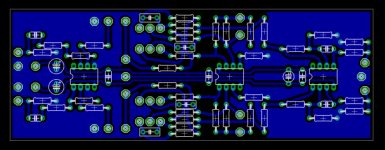
That looks pretty good to me. There is now more ground trace between ground connection points.
The only thing you haven't got is power supply decoupling capacitors next to the op-amps. USUALLY, op-amps work better if there are capacitors between their supply rails and ground, close to the op-amp. For example, 1uF solid tantalum electrolytics have good bandwidth and small size and would fit on your pcb. I am not familiar with the op-amp you are using.
It may be that Rod Elliott has a good reason for not having these. Or he may have overlooked this. You need to ask him.
- Status
- This old topic is closed. If you want to reopen this topic, contact a moderator using the "Report Post" button.
- Home
- Amplifiers
- Solid State
- Please comment my PCB!