am trying to current boost the lm317 to make agood bench ps.
iused amedium power BJT (BD140) for biasing, idont know how
to calculate the appropraite resistor value for the base so iused a
variable 100k. , it just worked as theres no BJT atall, imean the normal
operation of the lm317,, how do i make it work and to calculate
the proper value for resistor so ican decide the exact value of current
inwhich the BJT start conducting the excess current..
thanks all.
Attachments
I think you need to understand how it works first.
The resistor you want to know doesn't even need to be there and the one that is needed is missing and shoud be between emitter and base which would provide the voltage drop needed to switch the transistor on when the current reaches a certain value. Perhaps use something else than the BD140 as it is unsuitable for the task.
I strongly suggest reading any of the datasheets available for this type regulator as these deal with the current boost.
Actually the datasheet contains the same type setup in the later pictures but along with current control (which is not a bad thing to have).
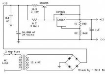
Check this for variations closer to yours:
http://ourworld.compuserve.com/homepages/Bill_Bowden/page12.htm
Check this for variations closer to yours:
http://ourworld.compuserve.com/homepages/Bill_Bowden/page12.htm
itook the 2nd schematic already from that page u posted,,
iput about 20ohm resistor bet. emitter and base as u said , but ifound
astrange thing actually, when i measured the current passing from
collector to lm317 output pin, then measured the total load current
ifound out they're the same... am sure that the regulator is the working one as it dissipates much heat,, so?!
am confused..
The second diagram shows two resistors, 0.3 and 0.7 ohms. Which of these is your 20 ohm resistor? And what is the other value that you are using? How much current did you measure, and how did you measure it? You can measure the voltage across these two resistors and calculate the current from that.deepanger said:itook the 2nd schematic already from that page u posted,,
iput about 20ohm resistor bet. emitter and base as u said , but ifound
astrange thing actually, when i measured the current passing from
collector to lm317 output pin, then measured the total load current
ifound out they're the same... am sure that the regulator is the working one as it dissipates much heat,, so?!
am confused..
Answer these questions and someone out there will be able to help. Or draw a diagram of exactly what you've built and post it, even better.
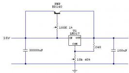
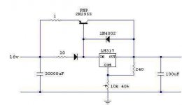
ididnt use any of those 2 schematics,, iused the 1st one i posted and
it didnt work as ive put the resistor in the wrong place, so itried
the right thing (aresistor bet. emitter & base) , and ive found that
the BJT isnt working although theres acurrent flowing from collector
to the output (used an ammeter bet. collector and output pin of the
regulator),, ican find that only the regulator is working in its normal
operation like as theres no BJT at all..
heres the current schematic i use:
Attachments
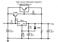
If boosting the current output of the LM317, while still keeping the regulated voltage is your goal, then you should use the LM317 to drive another transistor. The LM317 regulator sould be connected so that the OUTPUT of the LM317 goes to the base of an NPN transistor. The collector should be connected to V+, and the emitter is the new output, just like an emitter follower circuit. The LM317 adjustable voltage regulator now only has to drive enough current to operate the transistor, Ic/Beta. If you use a 2N3055, the LM317 shouldn't have any trouble driving this transistor without a heatsink. The transistor may require one though.
"while still keeping the regulated voltage is your goal, "
Congrats, you have just degraded to the functional equivalent of a pass transistor and a zener in the base.
Use the diagram with the 2955 pass transitor and ditch the BD140. Add a diode in series with the 0.7 ohm resistor. The ratio of current between the regulator and the pass transistor will now be the ratio of the two resistors. I suggest about a 5:1~10:1 ratio, meaning a 0.1 on the 2955 and a 0.5 on the regulator, or a 0.1 on the 2955 and a 1 on the regulator.
djk said:"while still keeping the regulated voltage is your goal, "
Congrats, you have just degraded to the functional equivalent of a pass transistor and a zener in the base.
Use the diagram with the 2955 pass transitor and ditch the BD140. Add a diode in series with the 0.7 ohm resistor. The ratio of current between the regulator and the pass transistor will now be the ratio of the two resistors. I suggest about a 5:1~10:1 ratio, meaning a 0.1 on the 2955 and a 0.5 on the regulator, or a 0.1 on the 2955 and a 1 on the regulator.
so if ive acurrent of 0.8A passing through the regulator ill ve 8A passing through the BJT. is it that simple or am confused?!
u mean it to be this way..
Attachments
"so if ive acurrent of 0.8A passing through the regulator ill ve 8A passing through the BJT. is it that simple or am confused?!"
It is that simple!
In an actual circuit if you needed 8A I would use two 2N2955 and keep the emitter resistors small. If you actually ran 8A with a single 1 ohm resistor the power in the resistor would be 64W!
"u mean it to be this way.."
Your diagram looks good other than the resistors need to be a bit smaller as discussed, and the 1N400X diode needs to go from the 100µF cap to the 30000µF cap. The function of this cap is to prevent the 100µF from discharging into the output pin of the regulator (which would damage it).
I built a couple of 13.8V 50A regulators (for car stereo) using this circuit, it works well.
"Not excactly, the 317 IC does have an error amplifier within. One way or another"
It certainly does, but driving the base of an NPN pass transistor from the output of the regulator disables it. The circuits in the various National Semiconductor Handbooks really are the best, and they generally give enough theory to allow you to modify them (within reason).
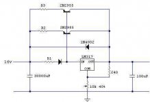
That looks good.
I would try 0.1R 3W for R2, R3, and around 0.82R 1/2W for R1, this would be about 4A through each of the pass transistors and 0.5A through the 317.
You may need to add a 0.33µF film cap on the input pin for the 317 and a 0.1µF film cap on the output pin of the 317, as close to the device as you can get (to prevent oscillating).
A 10µF stacked film type would probably be better than a 100µF electrolytic at the output.
- Status
- This old topic is closed. If you want to reopen this topic, contact a moderator using the "Report Post" button.
- Home
- Amplifiers
- Solid State
- current boost lm317 prob.