I have a Sony TA-F555ES integrated amp. It had problems with the protection (which is now fixed), and of course I thought I'd set the bias and put it all back together.
Found the measuring points, and basically read '0.00V'. So I check the manual, and it says to adjust to read 100mV. So I start to crank it up slowly, and even as I got to a reading of about 50mV, I noticed waves of heat rolling off the heatsink... Wha..??
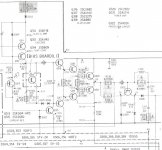
I turn down the bias to read about 1mV, and power off. I suspect that the collector resistor is not what Sony says. If you look at the collector resistor in the pic (R339), Sony has it labled '1 ohm 5W', so if indeed that was the value, 100mV would result in 100mA. But on examination, I see this dinky resistor the size of a normal 1/4W film resistor, and upon measuring it, it appears to be a 0.1 ohm instead of 1 ohm. No wonder 50mV was freaking it out...was pushing 500mA through it!! Luckily, nothing fried.
OK...so if it's really a 0.1 ohm, then set to read 10mV across it to get 100mA. So I set it, and the output transistors (2SC2922 & 2SA1216) get too hot to keep your finger on after just a minute or two, and the heatsink is shedding waves of heat too. Still confused, I drop the bias to where I read 1mV across the resistor. Set here, it gets fairly warm...not blistering, but a lot warmer than what you would expect if it had only 10mA of current through the outputs.
Almost all my amps are TO-3 output devices. On most of them they want a bias of about 50mA, and with that set, the heatsinks (even fairly small ones) get 'warm', and the transistors themselves 'feel' to a finger to be not a whole lot warmer than room temp. So these MT-200 devices getting as hot as they do with what is 'supposed' to be 10mA through them pretty much shocks me.
Another thing that's wierd...the size of the resistor. If it were indeed a 0.1 ohm 1/4W, it couldn't pass more than about 1.6A.... The color code on the resistor is tough to read buried where it is, but appears to be 'brown black gold gold'. Seems that would be a 1 ohm resistor, but a 250mW 1 ohm wouldn't last very long on the collector on the PNP device.
The parts list says it's a '1 ohm, 5%, 1/4W'. No way, even though that's what it appears to be. To confuse matters more, in the text where Sony is bragging about how wonderful this amp is, they say this:
I'm about ready to set the voltage drop across the resistor to 1mV and call it a day. But is there a possibility that it is a 0.01 ohm instead? With my meters (nice Fluke ones), I don't have the kind of resolution to measure values like that...
Opinions?
(sorry for the length...this is just wierd and I wanted to at least try to be clear..)
Found the measuring points, and basically read '0.00V'. So I check the manual, and it says to adjust to read 100mV. So I start to crank it up slowly, and even as I got to a reading of about 50mV, I noticed waves of heat rolling off the heatsink... Wha..??
I turn down the bias to read about 1mV, and power off. I suspect that the collector resistor is not what Sony says. If you look at the collector resistor in the pic (R339), Sony has it labled '1 ohm 5W', so if indeed that was the value, 100mV would result in 100mA. But on examination, I see this dinky resistor the size of a normal 1/4W film resistor, and upon measuring it, it appears to be a 0.1 ohm instead of 1 ohm. No wonder 50mV was freaking it out...was pushing 500mA through it!!
Luckily, nothing fried.OK...so if it's really a 0.1 ohm, then set to read 10mV across it to get 100mA. So I set it, and the output transistors (2SC2922 & 2SA1216) get too hot to keep your finger on after just a minute or two, and the heatsink is shedding waves of heat too. Still confused, I drop the bias to where I read 1mV across the resistor. Set here, it gets fairly warm...not blistering, but a lot warmer than what you would expect if it had only 10mA of current through the outputs.
Almost all my amps are TO-3 output devices. On most of them they want a bias of about 50mA, and with that set, the heatsinks (even fairly small ones) get 'warm', and the transistors themselves 'feel' to a finger to be not a whole lot warmer than room temp. So these MT-200 devices getting as hot as they do with what is 'supposed' to be 10mA through them pretty much shocks me.
Another thing that's wierd...the size of the resistor. If it were indeed a 0.1 ohm 1/4W, it couldn't pass more than about 1.6A.... The color code on the resistor is tough to read buried where it is, but appears to be 'brown black gold gold'. Seems that would be a 1 ohm resistor, but a 250mW 1 ohm wouldn't last very long on the collector on the PNP device.
The parts list says it's a '1 ohm, 5%, 1/4W'. No way, even though that's what it appears to be. To confuse matters more, in the text where Sony is bragging about how wonderful this amp is, they say this:
The resistance of the emitter resistor (authors note: there is no emitter resistor!!) used for the amp's bias network is 0.1 ohm, the lowest possible value which will keep the output stage stable and output distortion mimimum.
I'm about ready to set the voltage drop across the resistor to 1mV and call it a day. But is there a possibility that it is a 0.01 ohm instead? With my meters (nice Fluke ones), I don't have the kind of resolution to measure values like that...
Opinions?
(sorry for the length...this is just wierd and I wanted to at least try to be clear..)
Attachments
Hmmm... What an odd use of D305,D306 
Anyway... Is TP2 connected to the negative supply rail, or is there more to it than can be seen on the schematic section you've scanned?
What is the potential (rel. to GND) of TP1? It should be about
"-61V" according to the schematic.
I know it sounds nasty, but have you tried to un-solder R339 and connect an ampere-meter to the solder-spots in stead?
100 mA idle current is quite high for a class B amp (as they claim it to be), and it will cause quite some heat.
You could also try to switch the resistor to a new one which you KNOW is 1 ohm.
Jennice
Hi Echo
I think the the resistor is effectively a 0,1 Ohm 5 w resistor.
But it can be also a 1 Ohm resistor with 0,25 W that is only used for calibration purposes and after calibration it must be shorted.
About the heat issue i suspect that the problem with your Sony is oscilation .
Regards
I think the the resistor is effectively a 0,1 Ohm 5 w resistor.
But it can be also a 1 Ohm resistor with 0,25 W that is only used for calibration purposes and after calibration it must be shorted.
About the heat issue i suspect that the problem with your Sony is oscilation .
Regards
Interesting thought, Tube Dude!
I didn't give it much thought that there is done nothing (nothing visible on the schematic shown, anyway) to prevent oscillation!
EchoWars,
Do you know someone with an oscilloscope? If so, bribe them to bring it to your house, or bring the amp to the scope, 'cause it'll really help you tracking the problem.
Jennice
It just looks funny because of the way Sony drew it...redraw with the diodes in the vertical, and it looks more normal.Jennice said:Hmmm... What an odd use of D305,D306
Yes...goes right to the supply cap.Anyway... Is TP2 connected to the negative supply rail, or is there more to it than can be seen on the schematic section you've scanned?
About the same as TP2...at the moment, I have the voltage drop across the resistor set for 1mV. Heatsink still gets a lot warmer than you would expect.What is the potential (rel. to GND) of TP1? It should be about
"-61V" according to the schematic.
I'm thinking about this, but the resistor is bloody difficult to get to. Thought I'd see what someone else thinks first, and maybe if anyone else has opened up one of these.I know it sounds nasty, but have you tried to un-solder R339 and connect an ampere-meter to the solder-spots in stead?
How to choose a value? The circuit description text says '0.1 ohm', but the schematic and the parts list say '1 ohm', and the schematic says '5W' but the parts list says '1/4W' (no way does a 1/4W 1 ohm resistor belong in there). If I replaced, I'd be tempted to put a 0.1 ohm 3W or 5W in there...or maybe a 0.5 ohm 5W (since I have a bunch of these around).100 mA idle current is quite high for a class B amp (as they claim it to be), and it will cause quite some heat.
You could also try to switch the resistor to a new one which you KNOW is 1 ohm.
Edit: Sure...got a nice Tek scope right here. No oscillation on the output, at least none that a 100MHz Tek can see.
Ok, here's another suggestion (assuming that you have ~0V DC on your output terminal).
Connect a sine generator to the input, and monitor the output.
Initially (at zero bias) you should have some cross-over distortion.
When you reach the point where this distortion is gone, does it still get hot (not caring what the exact idle current is?)
Jennice
Connect a sine generator to the input, and monitor the output.
Initially (at zero bias) you should have some cross-over distortion.
When you reach the point where this distortion is gone, does it still get hot (not caring what the exact idle current is?)
Jennice
DC offset sits about 0.1mV (it has a servo).
I tried your idea. I have a Tek 4084 distortion analyser, which has an output that allows you to view the output of the amp minus the input signal (in essence, the distortion component). On the scope, I can superimpose the signal with the distortion, and I've done this before to view crossover distortion (superimposing just helps to see where the distortion is occuring on the wave). However, even with a very low-level signal (where the crossover distortion ought to be more obvious) and the voltage drop across the resistor set to '0.00V', I see no crossover distortion whatsoever.
Odd...
I'm starting to get a bad feeling about this.
Have you checked that your transistors are intact?
I am concerned that your output stage has a faulty transistor, and is only kept in place by the DC servo.
As soon as the bias is turned up, the faulty transistor causes an abnormally high current to flow. Just a theory. Other than that, maybe a driver is shorted, making the thermal compansation inaccurate?
Jennice
I suggest temporarily soldering a 1 ohm 5W resistor in place of the unknown one, then adjusting bias and then placing back the old resistor
If there is enough space on the board, you may even leave the 1 ohm 5W resistor in the board and solder the old 'unknown' resistor [or a piece of wire] to its legs in orden to ease further bias adjustments [just desoldering one side of the old resistor/bridge]
If there is enough space on the board, you may even leave the 1 ohm 5W resistor in the board and solder the old 'unknown' resistor [or a piece of wire] to its legs in orden to ease further bias adjustments [just desoldering one side of the old resistor/bridge]
Output trannies, drivers, and pre-drivers are good. Trust me on this one, I know. Plus, output looks just too good to be the result of an amp with transistor problems. When the only symptom is excessive heat and there's no oscillation, bias has to be the issue: just have to figure out where to set it.
I see no wire under the resistor, and yes, the Fluke does tend to tell me that it's a 0.1 ohm. I mean, it doesn't measure as a short...just close to one. And, of course, both channels measure the same in all respects...resistance values to power-on behavior.
Eva... What's the possibility that...the resistor in the amp now is a 0.1 ohm, and proper bias is when I get 10mV across it, and that the amp just runs really damn hot? I'm not used to output transistors in a Class B amp running almost hot enough to burn a finger (maybe a little bit of exaggeration, but they are certainly hot by any measure). What I think I'd find if I did what you suggested is that, with 100mA through the outputs, they'll be blazin' hot. Do these MT-200's just run that hot?
I dunno...maybe I should stick with the original plan...set for 1mV (what seems to be 10mA) and call it good. I cannot see or measure any crossover distortion, so I'm not ready to begin losing sleep over it.
Speaking of which, I badly need some. I'll check back later, but I really appreciate your inputs. Thanks guys!
I see no wire under the resistor, and yes, the Fluke does tend to tell me that it's a 0.1 ohm. I mean, it doesn't measure as a short...just close to one. And, of course, both channels measure the same in all respects...resistance values to power-on behavior.
Eva... What's the possibility that...the resistor in the amp now is a 0.1 ohm, and proper bias is when I get 10mV across it, and that the amp just runs really damn hot? I'm not used to output transistors in a Class B amp running almost hot enough to burn a finger (maybe a little bit of exaggeration, but they are certainly hot by any measure). What I think I'd find if I did what you suggested is that, with 100mA through the outputs, they'll be blazin' hot.
Do these MT-200's just run that hot?I dunno...maybe I should stick with the original plan...set for 1mV (what seems to be 10mA) and call it good. I cannot see or measure any crossover distortion, so I'm not ready to begin losing sleep over it.
Speaking of which, I badly need some. I'll check back later, but I really appreciate your inputs. Thanks guys!
Hmm....
I don't like your description of the amp's temperatures. It doesn't sound healthy to me.
Then again, Sony Amp's do tend to run hot. A friend of mine had a sony amp which worked perfectly well. I never really trusted it, though, as it was (even at idle) hot enough to smell that certain scent of hot air when breathing in over the amp (through the enclosure openings).
Could it really be the case that Sony Amp's are rice cookers?
Jennice
I think that brown-black-silver is 0.1 ohms and brown-black-gold is 0.01 ohms. Could anybody confirm this?
This resistor may be actually a fuse resistor to prevent disasters in case of shorted output devices
Heatsink overheating is obviously due to bias current being higher than expected, 100mA with 61V rails makes just 6.1W per output device. The only way to know the actual bias current is to temporarily replace the ?fuse? resistor with one of known value
Let's put some perspective in all of this.
The resistor according to the schematic is a 1 Ohm resistor.
According to the color bands Brown -1....Black- 0...Gold- X0.1...Gold-5% tolerance.
So the resistor must be 1 Ohm.
As the resistor, (as i stated in a early post) is only for measuring purposes. To be or not in circuit doesn't change the bias setting (because is in the collector circuit) .
So Sony ad NAD usually shunt this resistor after adjustment (for lowering the power supply impedance and limit the dissipation in the resistor)
So what Echo is measuring is the resistance of the short...0,1 Ohms.
If there is no wire under the resistance , then must exist a solder bridge or some point where the short is done.
If Echo take the resistor out of the circuit ,i bet that the resistor is a 1 Ohm one...and even with the resistor out of the circuit the short continue .
Cheers
In order to solve this mystery once and for all, I found a way to disconnect the negative power supply lead that runs to R339 and insert an ammeter. I also connected the voltmeter across the test points. On power up, there was 1.5V across the test points, and about 450mA (!!!!!!!!!) of current flowing!! I dropped the current to 100mA, and the voltage across the test points now measures about 0.3mV. Sure, that calculates to a resistance of about 0.03 ohms, but measuring a voltage that low isn't too accurate, so I suspect that the resistor is a 0.01 ohm.
Wierd. Certainly no wonder the amp was trying to go up in flames with it set to 10mV. Also pretty funny that the manual says to set the voltage across the resistor to 100mV.
I dropped the current to 100mA, and the voltage across the test points now measures about 0.3mV. Sure, that calculates to a resistance of about 0.03 ohms, but measuring a voltage that low isn't too accurate, so I suspect that the resistor is a 0.01 ohm.Wierd. Certainly no wonder the amp was trying to go up in flames with it set to 10mV. Also pretty funny that the manual says to set the voltage across the resistor to 100mV.
Hi,
though this is an old thread, in case someone is fighting with this problem, I'll reveal the secret of the mystery bias resistor:
Tube Dude was right. There is a 1 ohm 1/4W resistor which is shorted during normal operation with a tiny jumper PCB soldered to the solder side of the main board across 2 poles near the bias resistor. So if you measure the voltage at the test points, you're actually measuring voltage loss over this wire!
When the jumper PCB is removed, the bias voltage can be adjusted to 100mV. My amp runs pretty cool after I set the bias correctly.
Before I found the jumper PCB, I set the voltage to 1mV. After removing the jumper, the actual voltage over this 1 ohm resistor was 250mV!
Aquarius72 said:Hi,
though this is an old thread, in case someone is fighting with this problem, I'll reveal the secret of the mystery bias resistor:
Tube Dude was right.
Thank you, Aquarius.
Like a Portuguese proverb say:
- Is better latter, than never ...
Cheers
very interesting how Sony sets the bias...
I got JVC RX-665 receiver with 1blown rear channel that use Sanken 2SB1560/2SD2390 Darlingtons (all 5 Ch) and the bias in the rear Ch is at around 1mA per trans and there is no way to adjust them.
The front Ch bias was @ 5-7 mA per trans. I run freq. resp. with 8 ohm spkr. using Clio and I couldn't believed what I found out:
@0.5 W there was a big dip of 4dB between 50-150Hz leveling to -0.5dB @ 400Hz
@2W the same thing but the dip was 2dB

Finally at around 5W things started to sort of look normal.
So I started to play with bias, running freq resp/2nd, 3rd Harm Dist. to see if I can get it flat. I almost cocked the sucker when the bias hit 100mA  I pulled back to around 25-30mA per trans, checked things again and the big dip was almost gone.
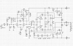
Still I have to see if the rears behave like fronts , it is one weird design . I copied the rear Ch onto CAD from the faulty PC board - hope its OK. What do you people think of it ?
Paul
I got JVC RX-665 receiver with 1blown rear channel that use Sanken 2SB1560/2SD2390 Darlingtons (all 5 Ch) and the bias in the rear Ch is at around 1mA per trans
and there is no way to adjust them.The front Ch bias was @ 5-7 mA per trans. I run freq. resp. with 8 ohm spkr. using Clio and I couldn't believed what I found out:
@0.5 W there was a big dip of 4dB between 50-150Hz leveling to -0.5dB @ 400Hz
@2W the same thing but the dip was 2dB
Finally at around 5W things started to sort of look normal.
So I started to play with bias, running freq resp/2nd, 3rd Harm Dist. to see if I can get it flat. I almost cocked the sucker
when the bias hit 100mA I pulled back to around 25-30mA per trans, checked things again and the big dip was almost gone. Still I have to see if the rears behave like fronts
, it is one weird design . I copied the rear Ch onto CAD from the faulty PC board - hope its OK. What do you people think of it ? Paul
Attachments
Hey, Aquarius72, thank You for clearing this mystery. You really helped me.Hi,
though this is an old thread, in case someone is fighting with this problem, I'll reveal the secret of the mystery bias resistor:
Tube Dude was right. There is a 1 ohm 1/4W resistor which is shorted during normal operation with a tiny jumper PCB soldered to the solder side of the main board across 2 poles near the bias resistor. So if you measure the voltage at the test points, you're actually measuring voltage loss over this wire!
When the jumper PCB is removed, the bias voltage can be adjusted to 100mV. My amp runs pretty cool after I set the bias correctly.
Before I found the jumper PCB, I set the voltage to 1mV. After removing the jumper, the actual voltage over this 1 ohm resistor was 250mV!
I know this is old thread, but anyway, can I ask You something? Can You also help solving the mystery about the V-I board DC BALANCE adjustment? Because, following the procedure from the service manual does not give any results. I believe there are also some steps omitted in the procedure, like it eas with the BIAS setting (omitted was a step for removing the jumper board before the adjusting to 100mV).
Here I put a thread:
http://www.diyaudio.com/forums/solid-state/205579-vintage-sony-ta-f555es-dc-adjustment-question.html
Thanks once again!
- Status
- This old topic is closed. If you want to reopen this topic, contact a moderator using the "Report Post" button.
- Home
- Amplifiers
- Solid State
- Overheating with low bias...