Ahh, what do I see, a XQ derivative! 
Ok, so you use S-"resistors", those 200 nH inductances in series in your schematic make me think you use a "one-turn" component commonly used by SMPS people, why do I think so?
Wouldn't you consider replace lower side FET's with IRF9540?
But you probably want to go the N-ch way anyhow...
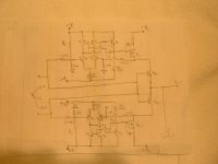
Your latest schematic is very complex, I'm thinking especially upper and lower CFP's which is not working the same way either.
You have double gain stages in your CFP, is that really good, at least the upper one?
The lower one consists partially of something looking like a folded cascode.
Cheers Michael
Ok, so you use S-"resistors", those 200 nH inductances in series in your schematic make me think you use a "one-turn" component commonly used by SMPS people, why do I think so?
Wouldn't you consider replace lower side FET's with IRF9540?
But you probably want to go the N-ch way anyhow...
Your latest schematic is very complex, I'm thinking especially upper and lower CFP's which is not working the same way either.
You have double gain stages in your CFP, is that really good, at least the upper one?
The lower one consists partially of something looking like a folded cascode.
Cheers Michael
Eva said:Would a single pair of IRF640 survive driving a 4 ohm reactive load (a bass horn) with +-40V rails provided enough cooling?
Ehmmm, in short - no. Maybe, assuming a non-reactive load and special care taken to cool the MOSFETs (like separate heatsinks so you can avoid mica insulators, and a copper core fan cooled heatsink. One of the most 'extreme' I've seen involved soldering a MOSFET onto a copper cored Athlon CPU cooler.
IRFP parts are MUCH better for this. Make a comparison of the IRF640 and IRFP240 for SOA, you will be amazed at the differences, although it's almost exactly the same silicon inside!
ilimzn:
That's a smart way to take advantage of the dissipation capabilities of MOS devices without messing with gate drive circuits and frequency stability issues as I did
Well, yes and no - it is not trivial, but it does work and makes a lot of things easyer. I can't claim it as mine, though - Sony uset that in some of their VFET (yes, the power JFET transistors again...) amps, but since the VFET is a depletion device, you only have to tie the gate to the output and you are set.
Ultima Thule said:Ahh, what do I see, a XQ derivative!
Ok, so you use S-"resistors", those 200 nH inductances in series in your schematic make me think you use a "one-turn" component commonly used by SMPS people, why do I think so?
What is XQ?
Those 200nH are just the estimated leakage inductance of a standard 0.25ohm wirewound resistor. Circuit behaviour at RF changes a lot when it's not considered
Anyway, PSpice is not going to show much of the actual circuit behaviour
Wouldn't you consider replace lower side FET's with IRF9540?
But you probably want to go the N-ch way anyhow...
It would be too easy this way, and N-ch and P-ch fets have very dissimilar transfer characteristics. Furthermore, both the direct and the inverting cell use the same number of transistors, so the circuit would look much like the same.
Your latest schematic is very complex, I'm thinking especially upper and lower CFP's which is not working the same way either.
You have double gain stages in your CFP, is that really good, at least the upper one?
The lower one consists partially of something looking like a folded cascode.
Cheers Michael
Yes, it's complex but I like it because all the complexity is made out of low-cost small signal devices and because it does not require any thermal compensation. In this last version with current sources I adjusted output stage bias current to 100mA with +-18V rails while the heatsink was at 15ºC or so, then I measured it back later after playing for a while with +-24V rails and the heatsink too hot to be touched... Still 100mA
Altough both CFP cells are not identical, they both should show unity current gain. The upper one just mirrors the error current because it's required to do so
while the lower one uses a folded cascode for level shifting that has also inherent unity current gain, thus the same current level flowing through the 22 ohm emitter resistors is applied to the bases of the totem pole gate drivers. The AC voltage gain is set by the RC networks, and the DC voltage gain is... Very high 
The diodes in paralell with the gate resistors may seem a bit weird, but clipping recovery behaviour improves a lot when they are added. Note that 1N4148 types are very convenient for that purpose because they are slightly resistive
One of the things that I have to improve is the current sources of the lower gate drive cell, because the current through the 10k resistor is modulated when the lower rail is bootstrapped (near clipping). This causes the voltage drop across the 1N4148 diodes to change and in effect modulates the current sources, thus reducing linearity and gain.
Ilimzn,
what cascode voltages have you thought of?
For those who are interested NP holds an old patent for cascoded OP.
Eva,
X=cross Q=quad..
It's interesting to see you adopt the XQ into yor design!
Oh, yes of course both have the same current gain, or so.. but what I meant the CFP's have a huge and a bit different gain is the internal voltage gain, for instance Q 19 with Q36 formed as a CCS has huge gain.
Q17 has a bit more gain than Q18 due to R43, isn't that correct?
You said earlier:
But isn't this due to the folded cascode in the lower CFP cell, are you able to check the propagation delay for respective CFP cell?
Cheers Michael
what cascode voltages have you thought of?
For those who are interested NP holds an old patent for cascoded OP.
Eva,
X=cross Q=quad..
It's interesting to see you adopt the XQ into yor design!
Oh, yes of course both have the same current gain, or so.. but what I meant the CFP's have a huge and a bit different gain is the internal voltage gain, for instance Q 19 with Q36 formed as a CCS has huge gain.
Q17 has a bit more gain than Q18 due to R43, isn't that correct?
You said earlier:
..you mean Q7 & Q8, just trying to follow you here.The positive cell has less phase margin, maybe due to the current mirror
But isn't this due to the folded cascode in the lower CFP cell, are you able to check the propagation delay for respective CFP cell?
Cheers Michael
Ultima Thule said:Ilimzn,
what cascode voltages have you thought of?
It depends on several factors.
Depending on the output BJT and MOSFET used, you want to utilise their power dissipation capability the best you can. So, logically, you would be looking towards about half the rail voltage for an even split between BJT and MOS, but depending on parts selected (perhaps by some of the criteria below), you may want a different split - although, typically, it will be the MOSFET that will take the brunt of the dissipation due to second breakdown immunity.
Then, the above has to be adjusted taking into account the Vgs for the maximum output current and drop on the BJT emitter resistors, as the BJT will be seeing that much less C-E compared to the cascode voltage.
Further, you also need to adjust for BJT SOA - at maximum BJT current you want your C-E voltage to be below the value where the second breakdown limit is imposed. This will typically be something from a few V to perhaps 15-20V.
Finally, you need to ensure that the Vgs of the MOSFET remains below it's maximum permitted value when the BJT is driven into saturation, which for most MOSFETs limits you to 20V.
You may also want to limit the Vgsmax in order to provide a current limit (non-foldback). It is possible to limit this by selecting the cascode voltage, but that way it will be quite low (5-8V for VMOS).
All in all, for typical transistors you end with voltages between 5 and 20V.
Eva said:CBS240: Could you draw it? I don't understand the description.
Hi Eva,
I bread-boarded a circuit basically similar to this, but then I had to go work out of state for 3 months
 ,(7 weeks yet to go) so I have not had a chance to get any real experimentation done. Quite sure improvements could be made. However, I was able to keep the phase of the output from the FET right on top of the “audio” at 15Khz,(that was as fast as I could get my cheap P-O-S op-amp oscillator to go and still get a smooth, stable sine wave) but I’m sure it will go to 20Khz.(still don’t have a function generator
 ) If you just use the FET as a follower from the audio, there will be a large phase shift due to gate capacitance and the wave forms will not line up. Local feedback compensates for this. C1/C2 in my circuit was 4.7nf to stabilize oscillations, but I’m sure this is dependent on the devices used and may be better placed as well.
 V1 is regulated and V2 is high current, but around the same voltage. R sets a DC bias on Q1 so that DC x gain(10) = Vce of Q14. The audio amplitude will be the same as Vout, but with a DC component, Vce. I did not use the FET for full wave though, but used a lower drive supply and two rectifier diodes in a class G style, but I don’t see why it wouldn’t work for full wave. By keeping the Vce of Q14 lower but dynamic, the SOA isn’t such a factor to the BJTs. Personally I’m with you on using BJTs for linear operations over FETs. If the FET output is slightly non-linear here, it isn’t such a problem to the actual output as long as there is no significant HF components as they will pass right through the BJT.
BTW, check out FQH90N15, and FQA36P15 from Farchild.(http://www.Fairchildsemi.com) They are new and have quite extensive SOA.
I plan to get some of these when I return home....if that ever happens.Attachments
Ultima Thule:
Yes, I decided to adopt my own non-latching and non-phase-reversing version of the cross quad due to its linearity. Mine is biased with 1mA and has 68 ohm degradation resistors, so it can whitstand more than 100mV of input differential voltage while still producing a perfectly linear output current. With a global voltage gain of approx 33, this means that the output voltage of the amplifier may deviate more than 3.3V from the expected value without overdriving the LTP or forcng it to produce non-linear error signals. This may be clearly observed during clipping, as the LTP turns off and on progressively while providing a very smooth error signal to the VAS.
That overdrive feature is highly desirable in non-class-A amplifiers employing vertical MOSFET output devices due to the *miserable* linearity of these devices, particularly at high frequencies and in the zero current crossing region, that may lead to high frequency glitches. The LTP must try to correct that without being disturbed. Note that the current gain of the VAS is strongly reduced at HF due to R35 and C8, so during any output glitch it may also take even 1mA of error signal without being overdriven itself.
Also, what I call the positive cell is the one driven by Q17, and the negative is the one driven by Q18. Both provide unity current gain and very high voltage gain to the gate at low frequencies due to Q19/Q36 and Q20/Q22 acting as current sources. The main difference, I think, is that in the positive cell Q19 is driven by the base and working in common emitter, while Q22 of the lower cell is being driven by the emitter and working in common base. Also, the layout of the positive cell in the breadboard is a bit more clumsy, so this may be reducing phase margin.
Oh, by the way, I'm considering driving the output stage into fake class-A by keeping both gate drive cells biased all the time, this would be a great improvement to linearity. Since the emitter currents of Q17 and Q18 are almost constant at audio frequencies, thus yielding constant Vbe and voltage drop across the 22 ohm resistors, the task is somewhat simpler than with conventional bipolar output stages. Conceptually, it would be achieved with two voltage sources, one between the base of Q17 and the output, and other betweem the output and the base of Q18, that should provide a minimum voltage (adjustable) that increases alternatively in one or the other depending on the VAS sourcing or sinking current. This may produce longer cross-conduction spikes when recovering from clipping, though (currently they are just 1us long so they are harmless)
Yes, I decided to adopt my own non-latching and non-phase-reversing version of the cross quad due to its linearity. Mine is biased with 1mA and has 68 ohm degradation resistors, so it can whitstand more than 100mV of input differential voltage while still producing a perfectly linear output current. With a global voltage gain of approx 33, this means that the output voltage of the amplifier may deviate more than 3.3V from the expected value without overdriving the LTP or forcng it to produce non-linear error signals. This may be clearly observed during clipping, as the LTP turns off and on progressively while providing a very smooth error signal to the VAS.
That overdrive feature is highly desirable in non-class-A amplifiers employing vertical MOSFET output devices due to the *miserable* linearity of these devices, particularly at high frequencies and in the zero current crossing region, that may lead to high frequency glitches. The LTP must try to correct that without being disturbed. Note that the current gain of the VAS is strongly reduced at HF due to R35 and C8, so during any output glitch it may also take even 1mA of error signal without being overdriven itself.
Also, what I call the positive cell is the one driven by Q17, and the negative is the one driven by Q18. Both provide unity current gain and very high voltage gain to the gate at low frequencies due to Q19/Q36 and Q20/Q22 acting as current sources. The main difference, I think, is that in the positive cell Q19 is driven by the base and working in common emitter, while Q22 of the lower cell is being driven by the emitter and working in common base. Also, the layout of the positive cell in the breadboard is a bit more clumsy, so this may be reducing phase margin.
Oh, by the way, I'm considering driving the output stage into fake class-A by keeping both gate drive cells biased all the time, this would be a great improvement to linearity. Since the emitter currents of Q17 and Q18 are almost constant at audio frequencies, thus yielding constant Vbe and voltage drop across the 22 ohm resistors, the task is somewhat simpler than with conventional bipolar output stages. Conceptually, it would be achieved with two voltage sources, one between the base of Q17 and the output, and other betweem the output and the base of Q18, that should provide a minimum voltage (adjustable) that increases alternatively in one or the other depending on the VAS sourcing or sinking current. This may produce longer cross-conduction spikes when recovering from clipping, though
(currently they are just 1us long so they are harmless)Thiese are the open loop gain/phase plots that PSpice predicts:
The O/L gain is flat up to 10Khz and the phase shift at that frequency is 90 degrees. Then, the gain is quickcly rolled-off at a 9db/oct slope thank to the pole plus pole/zero compensation. Closed loop gain is 30dB, so phase margin appears to be 60 degrees as the cursor shows, and all the audio band is kindly subject to 60dB of negative feedback. This was simulated in the crossover region, with 100mA bias, thus both gate drive cells working to compensate the very low gain of the MOSFETs at low currents.
It may look too optimistic, but the prototype is stable with these compensation networks. It doesn't ring when entering or coming out of clipping, being that a proof of good stability and phase margin.
p.s.: For all those subjectivists out there, it sounds just fine
An externally hosted image should be here but it was not working when we last tested it.
The O/L gain is flat up to 10Khz and the phase shift at that frequency is 90 degrees. Then, the gain is quickcly rolled-off at a 9db/oct slope thank to the pole plus pole/zero compensation. Closed loop gain is 30dB, so phase margin appears to be 60 degrees as the cursor shows, and all the audio band is kindly subject to 60dB of negative feedback. This was simulated in the crossover region, with 100mA bias, thus both gate drive cells working to compensate the very low gain of the MOSFETs at low currents.
It may look too optimistic, but the prototype is stable with these compensation networks. It doesn't ring when entering or coming out of clipping, being that a proof of good stability and phase margin.
p.s.: For all those subjectivists out there, it sounds just fine
Ultima Thule said:Ilimzn,
thanks for your detailed answer, as always an excellent teacher!
No
not a teacher but I have been told many times I should have been one
So if I got you right you would due to the explanation given use a fixed cascoding voltage 5 and 20 volts for the cascoded BJT, right?
Cheers Michael
Yes, the voltage is constant. A bootstrap cap with zener in parallel will work just fine, and depending on actual parts used and criteria as I explained above, you end up with a zener voltage of somewhere between 5 and 20V.
First, I have solved the issue of the cross-conduction spikes when coming out of clipping, I think. I used a stupid compensation trick that I will explain later.
Second, I decided to use the old VAS transistor BF471 as a cascode and put a BC546B with a constant Vce of 4.5V in its place. I increased the negative rail bootstrapping from 5V to 9V in order to provide enough voltage for Q18. PSpice must have gone crazy or something, because now it says that my circuit has 125dB open loop gain and still keeps 98dB at 10Khz... The real prototype now shows slightly improved phase margin even with lighter compensation, and the problem of oscillation that I previously had when the lower rail was bootstrapped is fully solved now, even without the RC filter that I was previously applying to the bootstrap voltage (33ohm and 330nF). Apparently, the non-cascoded VAS was not liking to be bootstrapped during the last 5V of the output swing, while the cascoded doesn't mind.
And third, I have tried all the suitable output transistors that I had at hand:
IRF640 - 200V 18A 0.18ohm 1200pF
IRF520 - 100V 9A 0.27ohm 350pF
IRF540 - 100V 28A 0.077ohm 1700pF
IRFZ48V - 60V 72A 0.012ohm 2000pF
HUF75309 - 55V 17A 0.07ohm 350pF
HUF75344 - 55V 75A 0.008ohm 3200pF
SKP10N60 - NPT-IGBT 600V 20A 1.8Vsat 580pF
To my great surprise, all worked fine without any adjustment of bias current or frequency compensation networks. The higher capacitance models (IRFZ48V and HUF75344) showed slightly smaller phase margin while the rest showed more or less the same behaviour as with IRF640.
I have also a pair of IRFP450 and some IRFP460, but I can't insert these directly in the breadboard, so I'll have to find out a way to test them without using wires (stability!!!). I'm thinking about soldering small pieces of resistor legs to the thick TO-247 pins in order to fit them in the TO-220 spaced breadboard holes.
As it can be seen, the circuit may be complex, but it is capable of readily producing sound from any gate driven device, even SMPS switching IGBTs!!!
By the way, I have observed up to 0.4V differences in gate threshold for 100mA between devices of the same batch and model... What a chore if I had to match them
Eva, several questions, if you don't mind
values of V2-V6?
why C1 and C21 are referenced to rails?
why C28, R64 and C5,R28 are referencrd to rails?
what is the purpose of extra lag C20?
values of V2-V6?
why C1 and C21 are referenced to rails?
why C28, R64 and C5,R28 are referencrd to rails?
what is the purpose of extra lag C20?
yes, this is because your splitter Q25, Q17, Q18 is sensing voltage drop across R16,R17 and not Vgs.all worked fine without any adjustment of bias current
Attachments
dimitri said:Eva, several questions, if you don't mind
values of V2-V6?
why C1 and C21 are referenced to rails?
why C28, R64 and C5,R28 are referencrd to rails?
what is the purpose of extra lag C20?
yes, this is because your splitter Q25, Q17, Q18 is sensing voltage drop across R16,R17 and not Vgs.
Supply rails (V2, V3) are +-24V now. Gate cell supplies (V4,V5) are made with 9.1V zeners, 330hm resistors and 100u capacitors. V8 lower rail bootstrap source was made with a 5.1V zener, 1K resistor and 100u capacitor, but later increased to 9.1V when I added cascoding to the VAS.
C1, C21, C28, C5, etc... are referenced to the rails because the circuit does not have a power ground, it only has a "floating" signal ground (not decoupled to the rails) that I don't want to contaminate with any non-signal current. The speaker wire comes twisted with the +V and -V wires to the power supply, and the speaker ground is taken there instead. The signal ground is connected to the same point as the speaker ground in the power supply, thus it's a perfectly clean reference. Since all the speaker current and possible spikes flow through these three twisted wires, inductive coupling to small signal circuits is negligible.
thank you,
what about short circuit protection?
upper half if protected at 8-10A by two diodes para b-e of Q17 and R33, but this doesn't work for lower half.
I like the idea to use bc546/556 everywhere, but Q13, Q18 and four input devices should be high-voltage types
I also understand your desire to use your own X connection, but I believe it is not optimal for this application
D15-18 and R33-34 don't have any output current limitation effect, the purpose of the resistors is to control the transconductance at RF (the output stage oscillates without them) and the purpose of the diodes is to protect Q17 and Q18 by limiting their Ic to approx. 30mA when the output clips. However, given the placement of R16 and R17, it's really easy to add a classic SOA V/I limiter. The final version will have it.
Concerning my cross-quad derivative, it's a good alternative because the original circuit will latch up or show phase-reversal effects as the amplifier clips, thus being not practical for that application. My circuit does the same in a more practical way, since it shows flawless clipping behaviour. Note that an excelent degree of cancellation of Vbe effects over gm is obtained even when the currents across the transistors are not perfectly matched, because the d(Vbe)/d(Ic) derivative is what really maters, and around 1mA it's almost the same (no matter if a transistor conducts 0.95mA and the other 1.05mA).
Also, in the original cross-quad circuit the inner transistor is operating at Vce=1.4V while the outer operates at the rail voltage. This ruins the cancellation effect because the pattern of change of Vbe with Ic is absolutely Vce dependent, and one Vce is up to two orders of magnitude higher than the other. In my circuit, both transistors are operating exactly at the same Vce (and the same Ic), thus better correction is expected.
Concerning the BC546B/556B in the input stage, they are good up to +-55V rails or so (Vce=65V max.) and above that I would add cascodes placed half way between ground and the rails The only transistors subject to the full output swing are BF871 and BF872, that are rated at Vce=300V and biased to only 3mA, so they will work fine witn rails over +-100V, even without heatsink because these come in a TO-202 case and already have a small built-in one.
However, I don't like to experiment in breadboards witn +-100V rails because the effect of two component legs touching accidentally may be disastrous, that's why I use a +-18 or +-24 current-limited supply until I make a PCB version.
Concerning my cross-quad derivative, it's a good alternative because the original circuit will latch up or show phase-reversal effects as the amplifier clips, thus being not practical for that application. My circuit does the same in a more practical way, since it shows flawless clipping behaviour. Note that an excelent degree of cancellation of Vbe effects over gm is obtained even when the currents across the transistors are not perfectly matched, because the d(Vbe)/d(Ic) derivative is what really maters, and around 1mA it's almost the same (no matter if a transistor conducts 0.95mA and the other 1.05mA).
Also, in the original cross-quad circuit the inner transistor is operating at Vce=1.4V while the outer operates at the rail voltage. This ruins the cancellation effect because the pattern of change of Vbe with Ic is absolutely Vce dependent, and one Vce is up to two orders of magnitude higher than the other. In my circuit, both transistors are operating exactly at the same Vce (and the same Ic), thus better correction is expected.
Concerning the BC546B/556B in the input stage, they are good up to +-55V rails or so (Vce=65V max.) and above that I would add cascodes placed half way between ground and the rails
The only transistors subject to the full output swing are BF871 and BF872, that are rated at Vce=300V and biased to only 3mA, so they will work fine witn rails over +-100V, even without heatsink because these come in a TO-202 case and already have a small built-in one.However, I don't like to experiment in breadboards witn +-100V rails because the effect of two component legs touching accidentally may be disastrous, that's why I use a +-18 or +-24 current-limited supply until I make a PCB version.
I hate it...
That's pseudo-class-A stuff. It keeps the ouput devices always biased to an adjustable current level (R79 and R80) and there is another "AC cross-conduction" adjustment (R78). That reduces gate-charging spikes (the ones in Ic(Q17) and Ic(Q18)) to an absolute minimum. These waveforms also show the extreme non-linearity that MOSFET devices show in class-B at high frequencies, even in the harmless PSpice models with linear capacitances.
In PSpice it looks beautiful, as always...
An externally hosted image should be here but it was not working when we last tested it.
An externally hosted image should be here but it was not working when we last tested it.
That's pseudo-class-A stuff. It keeps the ouput devices always biased to an adjustable current level (R79 and R80) and there is another "AC cross-conduction" adjustment (R78). That reduces gate-charging spikes (the ones in Ic(Q17) and Ic(Q18)) to an absolute minimum. These waveforms also show the extreme non-linearity that MOSFET devices show in class-B at high frequencies, even in the harmless PSpice models with linear capacitances.
In PSpice it looks beautiful, as always...
traderbam said:
That's the most complicated amp circuit I have ever seen.
No, it's just the strong neonic collors in here schematic that makes it complex!
Eva,
OMG, what are you doing..
Ic Q17, 18 doesn't look very funny..
I have thought myself a lot regarding what I call "dynamic-class-A" (you call it pseudo-class-A, don't know what is the correct name for it), I believe the transistion from the sustain to active region must be made softer to prevent such current jumps.
Cheers Michael
- Status
- This old topic is closed. If you want to reopen this topic, contact a moderator using the "Report Post" button.
- Home
- Amplifiers
- Solid State
- Reinventing the N-channel wheel?