Ultima Thule said:
No, it's just the strong neonic collors in here schematic that makes it complex!
Eva,
OMG, what are you doing..
Ic Q17, 18 doesn't look very funny..
I have thought myself a lot regarding what I call "dynamic-class-A" (you call it pseudo-class-A, don't know what is the correct name for it), I believe the transistion from the sustain to active region must be made softer to prevent such current jumps.
Cheers Michael
I'm just experimenting, measuring, playing and enjoying
For example, I have been looking at VAS emitter current waveforms (in the real prototype) with Q18 only used as a driver, and with Q42 as a driver cascoded with Q18 (Vce=5V). The latter case requires a more sine-like VAS current waveform to produce a sine amplifier output, thus it's clearly more linear and it wins.
I have been also looking at LTP collector current waveforms (also in the real prototype) with a single transistor VAS (Q15) and with a cascoded VAS (Q15 and Q40) with Vce=5V. Here, the difference is even more evident, the "gain" of the non-cascoded VAS is clearly modulated by Vce, while the cascoded VAS has a higher gain and requires a much more sine-like drive current in order to produce sine output.
So I have adopted both cascodes.
Ic of Q17 and Q18 just reflects the extreme non-linearity of MOSFETs (even considering that that my PSpice simulates constant capacitances). There are essentially two ways to linearize the amplifier, one is throwing the damn MOSFETs in some SMPS where they should have been always sitting and use some Sanken or Toshiba bipolars, and the other is finding a circuit having a non-linearity complimentary to the quadratic law of MOSFETs
I could produce a more smooth transition, but it would be only cosmetic, because the transfer function of the MOSFETs would be still here and the harmonics generated would be lower (currently they are essentially above 10Khz).Also, with bipolars the transition from the sustain region to the active region is much less troublesome and may be sharp because they behave more or less like constant current gain devices. I could drive the MOSFETs with symmetric gate waveforms around a center bias voltage (like I did in the schematic in page 1) but then there is a big issue: Vgs threshold not only changes with temperature but also with Vds!! This means that the bias is only constant when the zero-current transition happens at 0 volts. When driving reactive loads, there will be both excessive cross-conduction and crossover distortion due to a lack of bias depending on the voltage level where the zero-current transition happens (this is one of the reasons why people has to use a dozen TO-247 MOSFETs to make just a 500W amplifier, and that's something that I'm trying to avoid).
dimitri:
I have mailed you, but I got no reply
bigpanda:
Is this easier to read?
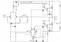
This is a fixture of my amplifier without global negative feedback. The signal coming from the output is bypassed with 100uF to ground that in turn forms a 0.16Hz low-pass filter with the 10K resistor. Only output DC level is corrected. The gain of the input LTP has been reduced by increasing the value of the degeneration resistors to 560 ohms, and the same has been done to the VAS forcing it to show unity current gain by increasing C8 to 470uF and loading its output with 22K to ground. With these modifications, an open loop gain similar to the closed loop value (30dB) is achieved.
This is how the actual prototype (configured as the previous schematic shows) puts a 10Khz sine wave at almost full power into a 2.5 ohm load (approx 70W). CH1 is input and CH2 is output. Note the ridiculous phase shift and the absence of visible distortion (PSpice predicts 0.6%):
When zooming with the oscilloscope, some mild crossover distortion may be observed, but there are not any spikes, even with bias levels as low as 10mA. The simple comparison of both waveforms also shows traces of some 2nd harmonic (asymmetry). I have measured the output impedance to be between 0.26 and 0.27 ohms, dominated by the 0.25ohm current sense resistors (and also the own lousy contacts of the breadboard), so the output stage itself does an excelent job by converting the 22K input impedance from the LTP to a few miliohms while taming all the MOSFET non-linearity (I'm currently using a pair of IRF540).
I'm considering placing some jumpers in the final PCB to allow to quickly change between an amplifier with 140dB open loop gain at 1Khz and an amplifier with 30dB of gain and no global feedback
I have to admint that I find quite difficult to distinguish both configurations by ear (but it has been demonstrated that most people will fail 50% of the times in a serious A/B test anyway ). The non-global-feedback version may interact a bit with the speaker (single 6" driver in a sealed box) by slightly attenuating midrange, but this is due to the 0.25 ohm output impedance.
p.s.: I have been too lazy to test the pseudo-class-A version with real components, but the non-global-feedback version was just much simpler to try
I have mailed you, but I got no reply
bigpanda:
Is this easier to read?
An externally hosted image should be here but it was not working when we last tested it.
This is a fixture of my amplifier without global negative feedback. The signal coming from the output is bypassed with 100uF to ground that in turn forms a 0.16Hz low-pass filter with the 10K resistor. Only output DC level is corrected. The gain of the input LTP has been reduced by increasing the value of the degeneration resistors to 560 ohms, and the same has been done to the VAS forcing it to show unity current gain by increasing C8 to 470uF and loading its output with 22K to ground. With these modifications, an open loop gain similar to the closed loop value (30dB) is achieved.
This is how the actual prototype (configured as the previous schematic shows) puts a 10Khz sine wave at almost full power into a 2.5 ohm load (approx 70W). CH1 is input and CH2 is output. Note the ridiculous phase shift and the absence of visible distortion (PSpice predicts 0.6%):
An externally hosted image should be here but it was not working when we last tested it.
When zooming with the oscilloscope, some mild crossover distortion may be observed, but there are not any spikes, even with bias levels as low as 10mA. The simple comparison of both waveforms also shows traces of some 2nd harmonic (asymmetry). I have measured the output impedance to be between 0.26 and 0.27 ohms, dominated by the 0.25ohm current sense resistors (and also the own lousy contacts of the breadboard), so the output stage itself does an excelent job by converting the 22K input impedance from the LTP to a few miliohms while taming all the MOSFET non-linearity (I'm currently using a pair of IRF540).
I'm considering placing some jumpers in the final PCB to allow to quickly change between an amplifier with 140dB open loop gain at 1Khz and an amplifier with 30dB of gain and no global feedback
I have to admint that I find quite difficult to distinguish both configurations by ear (but it has been demonstrated that most people will fail 50% of the times in a serious A/B test anyway
). The non-global-feedback version may interact a bit with the speaker (single 6" driver in a sealed box) by slightly attenuating midrange, but this is due to the 0.25 ohm output impedance.p.s.: I have been too lazy to test the pseudo-class-A version with real components, but the non-global-feedback version was just much simpler to try
eva, pls check your mail
so you lowered the gain by 110 db, lets compose a gain budget
- lowered transconductance of the first stage from 68 Ohm to 560 Ohm -20dB
- lowered VAS load from 1M to 22K -35dB
- before the input stage load was 68*hFE, now it is 68, assuming hFE=200 -46dB
-20-35-46=-100dB
ok, close by to 110dB
the input stage gain is -20dB, do you need it at all?
with 140dB open loop gain at 1Khz and an amplifier with 30dB of gain
so you lowered the gain by 110 db, lets compose a gain budget
- lowered transconductance of the first stage from 68 Ohm to 560 Ohm -20dB
- lowered VAS load from 1M to 22K -35dB
- before the input stage load was 68*hFE, now it is 68, assuming hFE=200 -46dB
-20-35-46=-100dB
ok, close by to 110dB
the input stage gain is -20dB, do you need it at all?
As SKA, your VAS-less circuit relies somewhat on constant gate capacitances (an additional gain stage makes it far better than SKA) and very strongly on constant Vgs/Id characteristics of the output devices across the entire output voltage swing for proper dynamic bias setting. But these characteristics are far from constant (simulation won't show it but real life does). Also, your circuit relies strongly on proper thermal feedback from the heatsink for bias setting, but you don't show how this is achieved in your schematic. That's a complex task that will require a dozen or so of components, thus making it less simple.
Also, your circuit is conceptual because it neither shows transistor models, nor component values, nor the required frequency compensation networks in the gate drive cells, nor input stage cascoding, nor the required thermal feedback from the heatsink, while mine reflects a true working and ready-to-build prototype. This makes me wonder seriously whether you really have the thing working or you are just dealing with something purely conceptual, without any analysis of real prototype behaviour. Could you post pictures of something capable of producing sound without smoke? Could you post oscilloscope captures showing amplifier output at high frequencies and current waveforms from each output device showing no cross-conduction?
On the other hand, my circuit does not rely at all on transfer characteristics of output devices thus it's much more robust and fault-tolerant:
- It even works fine with a IRF540 100V MOSFET in one of the rails and a SKP10N60 600V IGBT in the other. Since each output device will have a gate-drive cell, no matching is required. You toss random devices on the board and the circuit works fine.
- There is no need to readjust the bias when output devices are changed, the circuit is able to keep the bias constant independently of gate thresholds and without any thermal feedback from the heatsink thanks to the current feedback output stage. You toss random devices on the board and the bias is still kept at the same value it was adjusted last time.
- As my previous post shows, it produces low distortion when operating without any global feedback, because the "complex" output stage linearizes the output MOSFETs/IGBTs/whatever to such an extent that it makes them appear to the front-end as ideal adjustable current sources. You toss random devices on the board, and the real circuit still produces less than 1% distortion and sounds fine with all the 90dB of global feedback removed (you can see the oscilloscope capture in my previous post).
Your circuit is simple, but it will misbehave or destroy itself in any of the previous circumstances. Simplicity is not always a good thing in PA amplifiers (except when it allows you to make more money by selling an unreliable thing claiming it to be reliable).
Have you tried it driving 10Khz full power into 2.5 ohms without any global feedback? I bet your output waveform is going to resemble very little to the input sine
Hi, EVA,
Nice design (although your colorfull cct is hard to see)
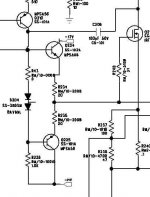
From your last schematic, you seems to make EC for each side. There are 3 loops in the whole amp. 1 loop is the main loop, by differential input pair. Upper side is controlled by CF loop by Q17. Lower loop by another CF loop by Q42, with folded cascode by Q22.
I want to ask about the final stage. If 1N4148 and BC's are having different B-E drop, would this force 1 side will have to saturate?
Why don't you make something like this?
How does it sounds?
Nice design (although your colorfull cct is hard to see
)From your last schematic, you seems to make EC for each side. There are 3 loops in the whole amp. 1 loop is the main loop, by differential input pair. Upper side is controlled by CF loop by Q17. Lower loop by another CF loop by Q42, with folded cascode by Q22.
I want to ask about the final stage. If 1N4148 and BC's are having different B-E drop, would this force 1 side will have to saturate?
Why don't you make something like this?
How does it sounds?
Attachments
Yes, you are right about the three amplifiers in one
At the beginning I also had doubts about the totem pole drivers biased with just two diodes. However, my pairs of 1N4148 biased to 3.3mA and my BC546B/BC556B combo resulted in a nice match because the transistors have a slightly higher Vbe than the diodes, so they always end up biased with just 100uA to 500uA, at the threshold of class-AB for small signal devices and with perfect thermal compensation.
I tried 1N4148 from two manufacturers and got the same results. The transistors are all On-Semi, though. I could insert a small resistor between the emitters just to be in the safe side, but I have very little space in the breadboard. I may put it in the PCB.
All my 1N4148s measure approx 630mV for 1mA, while the transistors show approx 680mV Vbe for 1mA Ic (at the same temperature).
Also, if you take a look at the datasheets of the transistors, you will see that the Vbe of the BC546B increases almost 80mV from Ic=1mA to Ic=10mA and the Vbe of the BC556B increases 50mV (for Vce=5V). That in fact works as if there were 8 and 5 ohm emitter resistors respectively, giving a great margin for diode tolerance and ensuring that excessive cross-conduction will hardly happen. In fact, I'm considering adding a small resistor in series with the diodes to intentionally increase cross-conduction and get better Ft and hFE.
To me it doesn't sound, it just amplifies the input waveform (Sound is a loudspeaker thing).
At the beginning I also had doubts about the totem pole drivers biased with just two diodes. However, my pairs of 1N4148 biased to 3.3mA and my BC546B/BC556B combo resulted in a nice match because the transistors have a slightly higher Vbe than the diodes, so they always end up biased with just 100uA to 500uA, at the threshold of class-AB for small signal devices and with perfect thermal compensation.
I tried 1N4148 from two manufacturers and got the same results. The transistors are all On-Semi, though. I could insert a small resistor between the emitters just to be in the safe side, but I have very little space in the breadboard. I may put it in the PCB.
All my 1N4148s measure approx 630mV for 1mA, while the transistors show approx 680mV Vbe for 1mA Ic (at the same temperature).
Also, if you take a look at the datasheets of the transistors, you will see that the Vbe of the BC546B increases almost 80mV from Ic=1mA to Ic=10mA and the Vbe of the BC556B increases 50mV (for Vce=5V). That in fact works as if there were 8 and 5 ohm emitter resistors respectively, giving a great margin for diode tolerance and ensuring that excessive cross-conduction will hardly happen. In fact, I'm considering adding a small resistor in series with the diodes to intentionally increase cross-conduction and get better Ft and hFE.
To me it doesn't sound, it just amplifies the input waveform
(Sound is a loudspeaker thing).How about using 3 diode drop, and small R for each emitors? This will bias the BC's all the time.In fact, I'm considering adding a small resistor in series with the diodes to intentionally increase cross-conduction and get better Ft and hFE.
In my experience, VBE of 1 kind of transistor will vary much. I've found difference of 0V61 to 0V67 for the same transistor type from the same manufacturer.
One more question. Why you use so much "soft clipping" cct ? Like Q12, Q45, Q46, D23 (not clear, upper left of D13)?
 box
box
Concerning three diode biasing, I will consider it for the PCB, because the breadboard is full now in this zone and redoing it is a mess
I use these current limiting approaches because, as this is not a standard topology, the devices being protected won't have any chance to saturate when clipping.
Q17 is protected by Q45, and Q19 by D... whatever , because otherwise this gate drive cell will enter into phase inversion and will oscillate during clipping. If the current is not limited, the Vgs of the output device will start to decrease after a certain current level is reached in Q45 due to the voltage drop that it will cause in R43 and R18 (limiting the amount of gate drive while more is asked). Also, allowing the small transistors to saturate deeply produces lousy clipping behaviour (oscillation).
The same happens with the VAS (Q40 and Q15) and Q18/Q42. These transistors are bootstrapped, thus they don't saturate during clipping, and the cascodes are rated at only 50mA but higher currents could be reached if no protections were adopted. Q46 also protects the B-E junction of Q22 from reverse breakdown.
As a result, clipping does not cause any stress on the circuit (I'm a bit PA-minded and I have seen a lot of equipment being abused and destroyed, sometimes I even had to repair it later, so good behaviour under severe overdrive is one of my goals). The circuit takes only a few microseconds to recover into full linearity.
I use these current limiting approaches because, as this is not a standard topology, the devices being protected won't have any chance to saturate when clipping.
Q17 is protected by Q45, and Q19 by D... whatever
, because otherwise this gate drive cell will enter into phase inversion and will oscillate during clipping. If the current is not limited, the Vgs of the output device will start to decrease after a certain current level is reached in Q45 due to the voltage drop that it will cause in R43 and R18 (limiting the amount of gate drive while more is asked). Also, allowing the small transistors to saturate deeply produces lousy clipping behaviour (oscillation).The same happens with the VAS (Q40 and Q15) and Q18/Q42. These transistors are bootstrapped, thus they don't saturate during clipping, and the cascodes are rated at only 50mA but higher currents could be reached if no protections were adopted. Q46 also protects the B-E junction of Q22 from reverse breakdown.
As a result, clipping does not cause any stress on the circuit (I'm a bit PA-minded and I have seen a lot of equipment being abused and destroyed, sometimes I even had to repair it later, so good behaviour under severe overdrive is one of my goals). The circuit takes only a few microseconds to recover into full linearity.
I seldom use base stopper resistors because my circuits are usually stable without them, and when I run into any oscillation issue I usually fix it with capacitors instead. Also, my VAS does not use the standard miller compensation (that may cause the output stage to interact with the VAS local feedback system and may require stopper resistors), instead it has a RC network in its base that fixes the current gain to unity at high frequencies (thus bypassing the VAS) and a small capacitive load that causes that output current to produce a rolling off voltage (a pole, plus a zero+pole form the RC network). It does not work in the same way as the single-pole conventional system.
As it was shown, this approach also produces low distortion when operated without any global feedback.
As it was shown, this approach also produces low distortion when operated without any global feedback.
Update:
I have been tweaking a bit the frequency compensation networks and that's what I finally got. This is how a 10Khz square wave driving a 10ohm resistor looks:
And this is a 100Khz square wave driving the same 10 ohm resistor. I had to reduce the voltage in order to prevent the resistors of the output HF dummy loads from toasting instantaneously:
I have been tweaking a bit the frequency compensation networks and that's what I finally got. This is how a 10Khz square wave driving a 10ohm resistor looks:
An externally hosted image should be here but it was not working when we last tested it.
And this is a 100Khz square wave driving the same 10 ohm resistor. I had to reduce the voltage in order to prevent the resistors of the output HF dummy loads from toasting instantaneously:
An externally hosted image should be here but it was not working when we last tested it.
All my oscilloscope captures are acquired from real prototypes with a HAMEG HM-407-2 in 100Ms/s digital storage mode, and transferred to the computer through RS-232. As I have mentioned several times through the thread, PSpice simulations of MOSFET linear circuits are of little use because most of the models available are almost ideal and doesn't even reflect non-linear capacitances, so they yield very inaccurate and optimistic results.
The amplifier prototype is currently breadboarded and a couple of pictures are shown in page 1 of that thread. Current schematic is similar to the last one that I published with minor changes (mostly to enable global feedback again after the crazy 10Khz open-loop test, and a 68pf phase-lead capacitor across the 10K feedback resistor).
The power supply is based in LM317 and LM337 and currently adjusted to +-24V. Practical DC current limit is 2A altough higher AC peaks are allowed due to storage capacitors. While this limits seriously the output power, it has prevented several disasters due to supurious contacts in the breadboard. The test loads are 10 ohm 50W power resistors with some heatsinking, that I combine to get other smaller values (2.5ohm, 3.3ohm, 5ohm).
The sine wave signals are generated through a computer sound card (either SB-AWE32 or VIA built-in chipset) and are bursted with a 10% duty cycle to allow testing with a 2.5 ohm load without folding the power supply. The square wave signals are generated with a battery-powered bread-boarded CD4049 CMOS hex-inverter configured as an oscillator, and since I can't use bursting here, test load has to be 10 ohm to avoid folding the small bench PSU (I have to build a decent generator one of these days).
Feel free to ask if you want more details.
Eva said:I have to build a decent generator one of these days
Seems to be common with you geenies.
Can you explain to a dork how you can get round using many OP devices on +/-90V, will forcing it in Pseudo-Class A not make it even more difficult ?
And the obvious: you intend to post the final layout for us to rob your IP ?
If you compare the pseudo-class-A schematic with the normal schematic, the difference is very subtle. The output stage is just the same, the only thing that changes is the class B splitter. My output stage works as two voltage controlled current sources, so the only thing that has to be done to keep it biased continuously is to provide a minimum drive voltage to the bases of Q17 and Q42 by means of two Vbe multipliers (that also compensate for temperature drift in Q17, Q42 and in the associated current sources of each gate drive cell). Anyway, I have serious doubts about the improvements that this solution could bring so I'm not likely to implement it.
To use higher rails I will obviously have to use more output devices. This brings two alternatives. One is to use matched devices with small additional source resistors and keep just two gate drive cells. The other solution is to use one gate drive cell for each output device and avoid completely the chore of matching, since each gate drive cell will drive each device to provide exactly the same current level, even when different models of output devices are employed In both cases the pseudo-class-A is implemented in the same way, since the bases of the "Q17" and "Q42" of each gate drive cell can be driven with the same bias setting voltage.
I've started to lay out a PCB with four gate drive cells. I want to know how much power can I get reliably from 4 TO-220 output devices.
Concerning other people copying my design... Well, it may happen. Actually I would be glad to see people building my stuff for personal use. Obviously, there are other people (salesmen) that are only focused on making profit from anything they get in their hands, but they already have their star producs and an enormous pride, so they are not likely to copy anything from me
To use higher rails I will obviously have to use more output devices. This brings two alternatives. One is to use matched devices with small additional source resistors and keep just two gate drive cells. The other solution is to use one gate drive cell for each output device and avoid completely the chore of matching, since each gate drive cell will drive each device to provide exactly the same current level, even when different models of output devices are employed
In both cases the pseudo-class-A is implemented in the same way, since the bases of the "Q17" and "Q42" of each gate drive cell can be driven with the same bias setting voltage.I've started to lay out a PCB with four gate drive cells. I want to know how much power can I get reliably from 4 TO-220 output devices.
Concerning other people copying my design... Well, it may happen. Actually I would be glad to see people building my stuff for personal use. Obviously, there are other people (salesmen) that are only focused on making profit from anything they get in their hands, but they already have their star producs and an enormous pride, so they are not likely to copy anything from me
- Status
- This old topic is closed. If you want to reopen this topic, contact a moderator using the "Report Post" button.
- Home
- Amplifiers
- Solid State
- Reinventing the N-channel wheel?