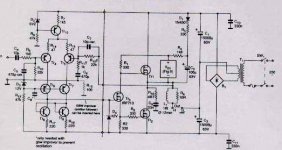
I've got a question. Why is in GM's type or JLH type output stage or non compliment type (like I attached here), they never use RE as emitor degeneration? Is RE forbidden in this type of output stage?
How if we wanted to parrarel the output stages, wouldn't RE is a must?
How if we wanted to parrarel the output stages, wouldn't RE is a must?
Attachments
if you want to add emitter resistors to balance the current in parallel output devices I don't see any difficulty - you would only be doing at the packaged transistor level what is implemented internally in many power transistor constructions
the real issue is whether you really want more power in a Class A amp; to accommodate impedance dips you might want 2x the nominal current bias giving 100 W continuous dissipation for 25 W rated output - 1 KW for 250W rms? - here it could be a "winter amp" - maybe you could run a Laundromat on the waste heat if you go 5.1 (looks like that should be a night-time amp with Bandung’s climate, maybe you could drive an absorption cooler during the day?)
the real issue is whether you really want more power in a Class A amp; to accommodate impedance dips you might want 2x the nominal current bias giving 100 W continuous dissipation for 25 W rated output - 1 KW for 250W rms? - here it could be a "winter amp" - maybe you could run a Laundromat on the waste heat if you go 5.1 (looks like that should be a night-time amp with Bandung’s climate, maybe you could drive an absorption cooler during the day?)
Why is that I get impression that many members here have been to Bandung?
JCX,
The thinking is simple. It's not about more power, but about safety. I got worries with hot transistors. They can act weirdly. 50W dissipation will be safer to be handled by 2 or 3 pair than 1 pair, right?
If you see the non-compliment article, the biasing method is quite different than GM's. GM is using bootstrap to upper rail, and non-compliment using fixed voltage referenced to output node.
Is these 2 resulting the same thing?
Hi Lumenauw.
You have attached the 'non-complementary' circuit due to Bengt Ollson, I think circa 1994, though there seems to be a drawing error for the pcb/heatsink split. It was class-AB.
Bengt went on to manufacture 250W.rms 8 ohms amplifiers using single push-pull pairs of output Mosfets with no emitter resistors. His solution regarding temperature compensation was in the little bootstrapped sub-circuit shown boxed beside TR1.
Two reasons for me to not like this circuit at the time were that it effectively had Miller compensation at the splitter driver, also it used a series output choke.
Bengt actually removed the choke in his next version, but increased Miller C with an additional component such that the phenomenal open loop gain started rolling off around 100Hz. Again I could not like that.
Bipolars need current bias; through base wrt emitter - in a JLH via the collector resistors and bootstrapped to the upper emitter.
Mosfets need voltage bias; to gate wrt source - Bengt also uses Vcc current flow, but voltage regulates and similarly bootstraps it to upper source.
Both lower output halves are already driven wrt to their emitter/source terminations, and the interposing of an emitter/source resistor here also increases the imbalance of the splitter drive wrt input stage output, though there is less effect upon a differential/mirror stage output.
________________________________________________________________
With correctly biased single output devices, emitter/source resistors actually degrade output stage performance, though they are essential for the correct hot running of parallel output devices.
Low value resistors do not degrade parallel performance however, due to the combined device decrease in effective emitter/source resistance.
_________________________________________________________________
JCX is of course correct relating to heat versus class-A power output, but modern devices are rugged, and your concerns can even more allayed by implementing a low drive resistance capable of quickly removing base/grid stored charges.
Cheers ............. Graham.
A question for Graham
In an amplifier with global feedback but with little or no compensation - the kind that you prefer
What would you think of as being an acceptably low propigation time
or to ask the same thing in a different way at what kind of frequency would you hope to see 1 degree of phase shift ?
I was thinking that 15 - 25 nano seconds was pretty good
What say you ?
mike
Hi Mike,
What a question !
The propagation time is more a function of the circuit, than what I might be looking for.
I look out for the way an amplifier reacts when simulated with a virtual loudspeaker, ie. I null the output at the virtual loudspeaker and study the error waveform and node currents with phase shifted crossovers. Thus the voltage output can be delayed wrt input, but the zero current crossover can arise several volts before the end of a first sine cycle, and non-class-A amplifiers always develop voltage crossover wiggles about that zero current crossover.
So it is not just propagation delay, but whether fully stable back emf induced error correction is completed. Any amplifier that can do all of this in say 50nS wrt first input base/gate is going to be excellent..
Cheers ............. Graham.
Hi there.
I'm in the middle of building the 25-8, and have a few question to the Zobel network:
1: Why choose 47nF + 2,2ohm instead of 100nF + 10ohm. Is it more "musical" due to the higher Fo??
2: Will it make any difference if placed at the speaker terminals instead of on the PCB??
Graham Maynard said:Hi Ejam,
My amplifier has a differential input stage which immediately makes it a different beastie to JLH designs.
The original JLH circuit is basically stable and as such did not need feedback compensation if sensibly constructed and used, but when modern high frequency transistors it might become necessary, with an output Zobel too. ( I use 47n and 2.2 ohms for mine where 100n and 10 ohms has been common.)
Cheers ....... Graham. [/B]
I'm in the middle of building the 25-8, and have a few question to the Zobel network:
1: Why choose 47nF + 2,2ohm instead of 100nF + 10ohm. Is it more "musical" due to the higher Fo??
2: Will it make any difference if placed at the speaker terminals instead of on the PCB??
I am afraid that Graham are not tracking our forum anymore.
He had some problems...some troubles inside our forum, someone that already disappeared from our forum had disturbed Graham`s mind and he gave up from our forum.
But i can remember that he said that this zobel filter values are something interesting to create a lower impedance patch into the earth, to avoid start of oscilations....as amplifier will be continuouly loaded related hi frequencies...... when starting oscilations the zobel will represent, in his design, something alike an enormous troat to drag those oscilations.
Depending of the source signal frequency, some oscilations could start, as he was using hi speed transistors and all them in the threshold of unstability, also Graham do not like Miller capacitors, and normally he used to avoid them, as those miller compensation capacitors normally turns sinusoidal input wave into triangle waves when frequency goes up into the spectrum...so, it can be a distorter too.
But as you know, Miller capacitor produces stability against oscilations too..... having not the Miller capacitor he decided that could be more safe make some modifications in the zobel filter values.
Graham continues to produce designs, but they are not published in our forum anymore, as he understood that bad educated guys can disturb, that no one will have protection, that we have only the forum rules that are not so strong to control those bad guys that sometimes appear in our forum...also that he is too much old to face those foolishes.... to see young boys, some of them without experience, some others with clearly bad intentions, to enter to discuss things already tested and that belongs to our Universal knowledge...things already accepted as true by almost half of our scientific world.
He is in some other forum...i heard that that forum collects people that do not accept this forum rules...well, i do not have the adress, as i accept almost all our forum rules...with some exceptions.
regards,
Carlos
Hi Carlos (destroyer X).
Thank You for the answer
I've been around for some years now, and yes, I've noticed the increasing amount of lack of respect and knowledge amongst some of the members who were the loudest, and that has kept me off for quite a while, not that I've suffered directly from their behaviour.
And I've also noticed that mr. Maynard has had more than his share.
A sad, sad story.
I'm very sad to hear that he has left "the building", but I can't blame him.
As I understand Your answer, mr. Maynards choise of component values is to avoid loading the circuit in the audible range, due to the higher Fo.
Is that correct ??
And now to my second question:
Will it make any difference if the Zobel network is placed at the speaker terminals instead of on the PCB??
I've had a curious experience with the circuit:
It starts to oscilate at @4MHz if the supply exceeds +/-10,5VDC.
That is without Zobel network, and connectet to an 50 ohm output from my HP 3325B function generator!!!!
Are You still happy with Your Maynard amp????
In the old days this Zobel network were placed in the speaker posts.
Now a days people are including it in the amplifier...to be more effective in the amplifiers point of view....well...the amplifier will be more happy to have this aid without the resistance, inductance and capacitance that will come from the speaker wiring.
I am not sure if will be better or not.
I used the Miller capacitor, the one that Graham do not want to be used.
Well...not to use it depends that you construct perfectly, avoiding too much wire length and other details....if not respected the construction practice suggested by Graham, i perceived, that the amplifier oscilated.....reason why i used the Miller capacitor in the voltage amplifier...from colector to base, as traditional.
Yes, i like his amplifier, i am still having it and i use it when i want to dream a little listening to music.
I hope he will come to help you, as i have not his knowledge, and i am not able to answer all the questions you may have.
regards,
Carlos
I had a conversations with Graham...and the result is here
Graham explained that is better to load output at RF, than degenerate *open loop* at AF !!!
Related the second question his answer was 'yes, it will make a difference'.
Also he explained that is essential to have a star output node at the amplifier circuit board
Bring the output transistor generated output to this node.
Zobel the node.
Take NFB from this node.
Drive loudspeakers from this node.
Graham said also that any other arrangement can lead to wire inductance interfering with NFB sense, drive or RF shunting being out of phase at HF.
Graham had moved on from that class-A, to better quality, better power and better efficiency. That old class-A is not completely stable.
He told that his new amplifier really is good, and one is presently running at 250W with Toshiba transistors !
He told also that will not return to our forum, also that he prefer the more close friends made using E Mails and suggested you, Dear Hoffmeyer, to follow this link.
He will not more cooperate, he made that because of me and you only….if someone need informs, please, follow the link.
http://www.zen22142.zen.co.uk/Circuits/Audio/gem100.htm
Carlos
Re: I had a conversations with Graham...and the result is here
Hi again
Just what I thought.
Sounds like I'm gonna redesign the PCB, and rewire the amp !
Very interesting link, and schematic.
My project is meant to inspire the electronic mechanics apprentices at my work, so the schematic will have to be fairly straight forward, like the 25-8, but I just might look into the GEM100 later
I'm honnored that mr. Maynard has taken the time to look into my questions.
The next couple of weeks will be spent looking for at house in Sweden, big enough to house my next speakerproject.
Coaxially folded exponentially 3½m back-loaded horn with a Fostex FE103E
But I'll be back with a progress report on the amp project
And thanks for Your answers.
Hi again
destroyer X said:Graham explained that is better to load output at RF, than degenerate *open loop* at AF !!!
Related the second question his answer was 'yes, it will make a difference'.
Just what I thought.
destroyer X said:Also he explained that is essential to have a star output node at the amplifier circuit board
Bring the output transistor generated output to this node.
Zobel the node.
Take NFB from this node.
Drive loudspeakers from this node.
Graham said also that any other arrangement can lead to wire inductance interfering with NFB sense, drive or RF shunting being out of phase at HF.
Sounds like I'm gonna redesign the PCB, and rewire the amp !
Originally posted by destroyer X
Graham had moved on from that class-A, to better quality, better power and better efficiency. That old class-A is not completely stable.
He told that his new amplifier really is good, and one is presently running at 250W with Toshiba transistors !
He told also that will not return to our forum, also that he prefer the more close friends made using E Mails and suggested you, Dear Hoffmeyer, to follow this link.
He will not more cooperate, he made that because of me and you only….if someone need informs, please, follow the link.
http://www.zen22142.zen.co.uk/Circuits/Audio/gem100.htm
Carlos [/B]
Very interesting link, and schematic.
My project is meant to inspire the electronic mechanics apprentices at my work, so the schematic will have to be fairly straight forward, like the 25-8, but I just might look into the GEM100 later
I'm honnored that mr. Maynard has taken the time to look into my questions.
The next couple of weeks will be spent looking for at house in Sweden, big enough to house my next speakerproject.
Coaxially folded exponentially 3½m back-loaded horn with a Fostex FE103E
But I'll be back with a progress report on the amp project
And thanks for Your answers.
Graham Maynard had visited our forum and he read all your posts
As he respect you Hoffmeyer, he is inviting you to go directly to his mail, and directly obtain all the informs you need.
You are welcome, not only because we know you for long time, an old forum friend, but also because we use to follow your posts and you are always kind, true, sensitive, decent and honest.
I just cannot publish his home mail, so, needing something, be confortable to write me, and then, i will put you, gladly, in contact with Graham.
I also feel myself very proud, as i could make very important friends, that meet me in direct mailing almost daily.
And you are beeing invited to join the Club.
nanabrother@yahoo.com
regards,
Carlos
Hi all
Models for the MJ21194 etc are matched to the data sheet, according to ON Semi. This means that as the data sheet usually represents the worst case, and as the avalanche breakdown usually only causes Ic to increase near BVce(x/r/o) often the Early voltage is far too low in these models.
John
Models for the MJ21194 etc are matched to the data sheet, according to ON Semi. This means that as the data sheet usually represents the worst case, and as the avalanche breakdown usually only causes Ic to increase near BVce(x/r/o) often the Early voltage is far too low in these models.
John
http://www.diyaudio.com/forums/showthread.php?postid=1383747#post1383747
Linux found the 649/669 here.
Linux found the 649/669 here.
All LTSpice transistor models have been obtained from files previously posted at here at diyAudio.
- Status
- This old topic is closed. If you want to reopen this topic, contact a moderator using the "Report Post" button.
- Home
- Amplifiers
- Solid State
- Graham's Class A/JLH output