Geoff said:Is it safe to assume that the current anomalies are generated by inaccurate models and that reality is closer to the simulation results obtained using Andy's revised model?
I wish I knew the answer to that
") . One thing that makes me suspicious is Figures 4 and 6 in the MJL3281A data sheet. The equations SPICE uses with the Early Voltage show that Figure 4 should be shifted upward from Figure 6 (beta increases as Vce increases). But there's so little change it makes me wonder whether this is a measurement error or the devices just don't fit the theoretical equations that well. Another technique for finding the Early Voltage is to look at Figure 8 and see where the linear part of the curves intersect the negative Vce axis. It's clear that they don't intersect at the same point, yet the Early Voltage theory says they should. In the end, I just guesstimated how much Figure 4 might be shifted upward relative to Figure 6 and came up with the 200 Volt number for VAF. I don't know if this really reflects reality. If figures 4 and 6 really reflect what the devices do at Vce = 5V and Vce = 20V, then the model should reflect operation in the circuit pretty well.
. One thing that makes me suspicious is Figures 4 and 6 in the MJL3281A data sheet. The equations SPICE uses with the Early Voltage show that Figure 4 should be shifted upward from Figure 6 (beta increases as Vce increases). But there's so little change it makes me wonder whether this is a measurement error or the devices just don't fit the theoretical equations that well. Another technique for finding the Early Voltage is to look at Figure 8 and see where the linear part of the curves intersect the negative Vce axis. It's clear that they don't intersect at the same point, yet the Early Voltage theory says they should. In the end, I just guesstimated how much Figure 4 might be shifted upward relative to Figure 6 and came up with the 200 Volt number for VAF. I don't know if this really reflects reality. If figures 4 and 6 really reflect what the devices do at Vce = 5V and Vce = 20V, then the model should reflect operation in the circuit pretty well.Using some of the 25W-8 features
Graham
Thanks for the reply. Two quick questions about using some of the features of your amp on the JLH amp. Talking about the JLH 1969 version modified for +/- power supplies. I think this is known as the Evolution modification as per Geoff's website.
First, could you use the 390 ohm emitter and 390 ohm collector loads for the driver transistor (2SC3421) with Rb = 270 ohms. Second, could you use the Rz modification, assuming the 2k7 and 220 feedback divider for DC offset stabilisation. Is feedback compensation needed here, you use 22pF but for this amp maybe 10pF? Output stage using the 2SC5200 and input stage using the 2SA970.
Anyone
If you could stimulate these mods, nice to know how they go. I suppose I like the idea of doing it with only four transistors...
Regards
Hi Andy,
Its great that you have managed to get 'Early Voltage' for Spice with On-Semi devices behaving more alike those of real life, and thus clarified Geoff's findings.
JCX's MJL3281A model must have had an EFV of around 20V for a 200V rated device; this does not make sense. Maybe there are other simulated amplifier designs that are not getting a second look because they too appear to behave worse than they actually do in real life.
Hi Ejam,
My amplifier has a differential input stage which immediately makes it a different beastie to JLH designs.
The original JLH circuit is basically stable and as such did not need feedback compensation if sensibly constructed and used, but when modern high frequency transistors it might become necessary, with an output Zobel too. ( I use 47n and 2.2 ohms for mine where 100n and 10 ohms has been common.)
To use 390 ohm output stage resistors the driver needs to have a higher level of linear current drive from the input transistor, also the four transistor design will always send a current wave through the loudspeaker as capacitors charge at start-up unless the bias is 'slugged'.
You mention the 2k7/220 ohm feedback resistors. These work fine but being in series with the first transistor emitter they degenerate first stage gain quite considerably.
'Doing it with four' is a decent challenge though, and thus I have enclosed this simulated circuit; i.e. not real-world tested. It does spec measure better than the original, but as in the old 'swings and roundabouts' saying, it might not actually sound better than those that have been hands+ears-on optimised via considerable user communication through Geoff's site.
Cheers ....... Graham.
Attachments
GM mod to the JLH Amp
Graham
Thanks for your efforts in "doing it" with only four transistors. The JLH reminds me of a Dyanco Stereo 70, input, concertina phase splitter and pp output stage. If it can be done with valves, why not with transistors!!
I must confess that there are a few oddities with the circuit. For example, the DC path of the feedback is linked to both the input transistor via the 680 ohm resistor and to the junction of the 390 ohm and 270 ohm of the bootstrap. There is a 1000uF cap across the pot and a 22pF compensation cap across the lot. Is the purpose of this arrangement to "slug" the bias on start up by feedback?
Also shouldn't the collector load of the input transistor (680 ohm) be to the negative rail rather than across the base - emitter of the driver transistor?
Would not the presented arrangement unbalance the driver transistor?
What happened to Rz and the RC zobel network?
Lastly I thought that the Gain Bandwidth Product of the input stage was fixed. Hence a lower gain results in a greater bandwidth. Given that the JLH is a low feedback amplifier, then less gain is required by all stages. Surely three stage of low gain, wide bandwidth and low feedback is preferable to three high gain, low bandwidth and high feedback. Regarding linear current driver, why not use an inherent linear high current transistor such as the 2SC3421.
Regards
Ejam
Hi Ejam.
I did as you asked, and get a load of questions.
Most four transistor JLH circuits do not need Zobels, I cannot know whether this one does until it is constructed.
The pot IS R.z and the 100uF is part of it. You can't load the output transistor base of the four transistor circuit.
Why does the first collector load need to go to ground, and how will this imballance driver input , this has high impedance for first collector and thus good first stage gain.
First stage gain and speed is limited by the high value 220 ohm emitter resistor in the original, hence my use of the lower value.
Remember low feedback means low damping, my circuit is better for complex loudspeakers.
I DO USE A 2SC3421 ?
Cheers .......... Graham.
No more questions but a few observations
Graham
As a novice but not a complete novice, the purpose of your feedback network was not obvious. Having stated in your earlier post that turn on was a problem for the JLH then I assumed that linking the network back into the bootstrap circuit which in turn is linked back to the positive rail was to avoid the turn on problems.
Second you use 10k as the Rz which is significantly different from the value of 100k to 1M that your amp uses. I think it is fair enough to ask where was R To me the 10k pot was adjusting the feedback.
You mentioned that the BC556B collector was to ground, where I asked why not to the negative rail.
Refering to the imbalance, if current is going thru BC556B then it flows through the 680 ohm resistor then thru the 390 ohm resistor where it joins the current flowing thru the 2SC3421. Hence you have more current thru the bottom 390 ohm resistor then you have thru the top 390 ohm resistor, hence an imbalance. Or does the 680 ohm resistor act as a bootstrap to the 2SC3421 to give a high input impedance to the 2SC3421? Normally bootstrap resistors have significantly higher resistance than 680 ohms.
You mentioned a 220 ohm resistor, where is that? Your modified JLH does not have a 220 ohm resistor.
I must apologise for writing "driver" instead of "drive" for the 2SC3421. I was refering to using the 2SC3421 for the input transistor rather than the BC556B.
I gather you are getting a little testie with my questions so I shalln't ask any more. Thanks very much for your help.
Ejam
Graham Maynard said:JCX's MJL3281A model must have had an EFV of around 20V for a 200V rated device; this does not make sense. Maybe there are other simulated amplifier designs that are not getting a second look because they too appear to behave worse than they actually do in real life.
That model, which is from the OnSemi web site, has an Early Voltage VAF of 46.776V. Looking at the characteristic curves of the device in Figure 8 of its data sheet, it's seen for the lowest Ib (0.5A) that:
Vce1 = 10V
Ic1 = 22A
Vce2 = 5V
Ic2 = 19A
Finding the intersection of this line with the negative Vce axis gives Vce = -VA = -36.7V, which is even lower than the 46.77V value in the OnSemi models. Yet if you simulate beta vs Ic at various Vce values with that Early Voltage value, the simulation would show that theres a significant increase of beta as Vce goes from 5V to 20V. But the data sheet shows that they are nearly identical (Figures 4 and 6 in the data sheet). For the data sheet characteristic curves (Figure 8), the lowest Ib is 0.5A, much greater than what's needed to compute the beta vs Ic curves, My only guess is that when the base current is small, the Ic vs Vce curves at a fixed Ib must intersect the negative Vce axis at a much more negative voltage value than they do at higher Ib values. So apparently the device doesn't conform well to the Early Voltage theory, which says they should all intersect the Vce axis at the same point.
Hi Ejam,
I am sorry, but you are piling on even more questions before you are thinking it out for yourself.
You think you are finding fault, but sadly you are wrong. Either build what I have suggested or simulate it so that you can come to understan the design.
The only problem I would be wary of is power supply and temperature change causing output potential drift, but that is what you get with a single input transistor, and why I changed to differential input which holds the output very accurately.
Cheers ............ Graham.
Hi Andy,
I have not taken a great deal of interest in Spice because I prefer to try circuits in real life. It is though an excellent comparative guide. Your figures are very interesting also.
It has been my past observation that JLH based amplifier circuits perform better in real life than Spice would suggest.
The Forward Early Voltage specification of models could have a bearing here, though as I have never studied Spice itself I did not know that it had the abreviation VAF. My simulator does not use these same abbreviations.
When I ran a few examinations I noted that the Reverse Early Voltage figure also affected the JLH output simulation. Is this abbreviated as VAR ? If yes, are the (different) figures quoted above in this string correct for a good modern 200V semiconductor ?
I mention this because a VAF of 46.776V on my simulator would be above the figure where the double humping effect becomes apparent with +/-20V output through 8 ohms from +/-25V rails.
Over to you, for I do not have experience here.
Cheers ............. Graham.
Re: Scaling Power Output to 10 - 12W
If you have good eficient speakers needing 15W, instead of a class A SS amp, I would build a tube amp, since you have much experience with valves. The sound quality will be much better.
Ejam said:Graham
I read your article and like the amp. I am from the valve school having build many amps but must confess ignorance when it comes to transistors. I would like to build a 10 - 12W version of your amp similar to the original JLH version. I have very efficient speakers and a small room and no need for the heat of the 25W version. My 8W 300B amp is more than enough. I would think that the rails of +/- 15V would be in the ball park. Can Tr5 be omitted if the amp rarely gets to maximum output ? Hope you can help with some suggestions.
Regards
If you have good eficient speakers needing 15W, instead of a class A SS amp, I would build a tube amp, since you have much experience with valves. The sound quality will be much better.
Hi Ejam,
You said a 'little testie', but actually I was very annoyed, and it has been bugging me as to why I became so.
I've just realised.
You posed those questions to me in a preceding negative form; i.e. 'should not so and so' or ' normally --- ' etc. thereby placing me in a position where either I had to agree with your statement (whatever its unstated origin) or explain otherwise ! If it 'should have been so and so' then there was also the implied assumption that I had either overlooked something or actually done something wrong ! I knew you were not a beginner from past postings and the questions themselves, so I also felt that you could have studied the circuit a little more before firing off so many questions.
I am strong on any individual being free to have their own slant on how a circuit works, and as to what they feel is most important for good audio. I see many views different to my own and am pleased for those differences, but I am also extremely firm that others should not expect me to think the same as they do or match a pre-conceived picture, for this is how big mistakes can and have been made throughout history, and how innovative development can become stunted.
I apologise for being a 'little testie', but I also trust that you can now understand why I actually became annoyed.
Cheers ......... Graham.
Hi Graham,
Congratulations on your article series in EW. The Sept. issue hadn't appeared locally yet as of last Saturday, but of course you've posted your circuit here. And, of course, I had a preview with the circuit you had sent me several months ago.
I noticed in the August article you seemed to come down very heavily on output capacitors. In a split-supply design, however, there are still capacitors in the signal path, so I don't see any getting around it. Or is it just relatively small capacitor values (< 4700 uF, say) that you are referring to?
A single-supply amp may be easier to implement, based on what power supply components are available. One thought I had was to build complementary amplifiers that could run from the +ve and -ve sides of an existing power supply that would otherwise have too high a voltage.
I'm quite keen to try your circuit. I'll need a suitable power supply first, however, so I hope to put together a test bed of sorts to try it, along with perhaps a more conventional JLH and an ESP DoZ (both of which I have partially started already).
Graham Maynard said:I have not taken a great deal of interest in Spice because I prefer to try circuits in real life. It is though an excellent comparative guide.
Understood. I work for a company that makes simulators (not any of the ones anybody uses here), so naturally I'm more interested in SPICE than most folks here are. Also, I come from the RF/microwave world, where not using a simulator is considered very unusual, since even simple gain calculations for those types of circuits can be intractable when done by hand. So it's just an engineering culture difference.
When I ran a few examinations I noted that the Reverse Early Voltage figure also affected the JLH output simulation. Is this abbreviated as VAR ? If yes, are the (different) figures quoted above in this string correct for a good modern 200V semiconductor ?
I mention this because a VAF of 46.776V on my simulator would be above the figure where the double humping effect becomes apparent with +/-20V output through 8 ohms from +/-25V rails.
Over to you, for I do not have experience here.
Yes, VAR is the standard SPICE name for the reverse Early voltage. I didn't change VAR from the OnSemi data, simply because I had no data on which to base a calculation. It's computed in a similar way to VAF, except the transistor is in the reverse active region, with collector-base forward biased, and emitter-base reverse biased. Since the device vendors don't seem to provide this data, I just left the values alone. I don't know what they should be.
In looking at the equations relating IC to VBE in Massobrio and Antognetti, the familiar expression from the Ebers-Moll model, namely:
IC = IS(exp(q*VBE/k*T) - 1) *K1*K2
has the two factors K1 and K2 tacked on, where:
K1 = (1 - VBC/VAF - VBE/VAR)
Note: VAF and VAR are defined as being positive, VBC is negative in the active region, and of course VBE is positive. I'll leave out K2 because the equations are too hard to write here. K2 involves high-level injection and is a function of IKF. The corresponding exponential expressions for IB vs VBE do not contain K1 or K2, so you can consider K1 and K2 as "beta scale factors". So it looks to me like VAR causes beta to drop off relative to its unscaled value as VBE increases (higher IC).
Also, I should mention another problem I had with the OnSemi model. Maybe it has some bearing on what you were seeing. I attempted to disable all current-dependent beta variations by removing IKF, which models the deviation of IC vs VBE from the ideal exponential function at high currents (reduced beta at high currents, or "high level injection"). Also, I removed ISE, which models the deviation of IB vs VBE from the ideal exponential at low currents (reduced beta in the low-current region). Strangely, the beta vs. IC curves still had a significant downward slope as Ic increased, even when I modified my test circuit to hold VCB, rather than VCE, constant . I finally tracked it down to an RC value that was way too large. At high currents, the internal collector voltage was dropping, and since the Early effect is derived from the internal VCB (which was dropping as IC increased), the Early effect when combined with the internal VCB drop was causing beta to decrease, even though I was holding the external VCB constant. I ended up changing the RC value from 0.2 Ohms to 0.06 Ohms. Then beta vs IC with VCE fixed looked flat. That was a frustrating problem!
Hi Paul,
It is not the 4,700uF series output capacitors I come down hard on, but the preconceived idea that they have no more impact upon reproduction other than to introduce a sub-audio -3dB roll-off.
So many early designs used 2,000uF and this upsets bass driver control, which is why I suggested EW readers should listen to the reproduction differences when different series capacitors are tried.
In a twin rail supply the capacitors are connected to the output devices and NFB ground reference, not introducing a complex voltage/current interaction between loudspeaker generated back EMF and the real NFB loop current controlled output voltage.
The beauty of all of these JLH based class-As is that they are easy to try, and will work from low voltages. A car battery will still give good output level.
Hi Andy,
I'm following that (just) and would like to point out something else that I've noticed with simulated audio power transistors, and which could be linked to your ISE removal.
The simulated V.be rises on dynamic waveforms with falling V.ce are much greater than in either real life, or the specification sheets suggest. This is bound to lead to different simulated dynamic and stability responses.
Cheers ...... Graham
Crossed wires
Graham
I guess my questions were taken the wrong way or I didn't explain myself with sufficient clarity, either way its not important. I find this type of communication (email) easy to get off on the wrong foot, particular when emailing people of different cultures. Trust me a five minute talk over the phone is so much better. As I said before I like your design much and my questions were not asked for you to prove your design against conventional wisdom but merely asking you to fill in some gaps in my knowledge concerning transistor design. I find interesting various points of view, in fact I encourage it in my students. I guess the trouble with audio is that "one man's meat is another's poison". Anyway I have your Electonics World design nearly complete and will test it over the weekend.
Cunningham
Have built many valve creations, just trying transistors for a lark. FWIW, triodes rule!
Regards
Ejam
Graham Maynard said:I'm following that (just) and would like to point out something else that I've noticed with simulated audio power transistors, and which could be linked to your ISE removal.
The simulated V.be rises on dynamic waveforms with falling V.ce are much greater than in either real life, or the specification sheets suggest. This is bound to lead to different simulated dynamic and stability responses.
Hi Graham,
I think it can be argued that this is the Early effect again. In the conditions you're referring to, you have Vbe varying and Vce varying. Let's try to hold something constant to simplify things, so let's assume for the sake of argument that Ic is being held constant. What really made the Early effect make sense to me was reading about how it's modeled in the simplest Ebers-Moll model. First, without considering the Early effect at all, and also assuming that beta is independent of current, the simplest equations for Ic and Ib as a function of Vbe in the Ebers-Moll model are the familiar exponential functions:
Ic = Is * (exp((q * Vbe) / (k * T)) - 1)
Ib = (Is / BF) * (exp((q * Vbe) / (k * T)) - 1)
or Ib = Ic / BF
so beta = BF at all currents. Putting in the Early effect changes only Ic vs Vbe, not Ib vs Vbe. So the first equation for Ic above becomes:
Ic = Is * (1 + Vcb / VAF) * (exp((q * Vbe) / (k * T)) - 1)
and the second equation above for Ib stays the same. If we were to plot ln(Ic) and ln(Ib) vs Vbe on the same plot, we'd get two parallel straight lines whose vertical separation is ln(beta), a so-called "Gummel Plot". An example is shown here http://people.web.psi.ch/palfinger/dipl/dipl/node26.html#labview_sat in figure 3.7 (this figure takes into account other non-ideal behaviors not mentioned above). When Vcb is varied, the upper curve (ln(Ic) vs Vbe) shifts up and down uniformly, but the lower one (ln(Ib) vs Vbe) does not budge! If Ic is held constant, the intersection of the horizontal Ic = constant line with the ln(Ic) vs Vbe line will change as Vcb is varied. Thus you'll end up with different values of Vbe for a given Ic, depending on what Vcb is.
Could ISE have an effect on this? I don't think it will, for the following reasons. ISE and NE model the dropoff of beta as the collector current becomes small. This modeling only affects Ib vs Vbe and not Ic vs Vbe. As you can see in the plot on the referenced web page, the dropoff of beta at low currents is due to Ib being greater than its ideal straight-line value at low Ic. That's the effect you see in the lower left of the graph. If we're assuming Ic = constant, this variation of Vbe that you see in your simulations is not affected by ISE or NE because those parameters only affect Ib vs Vbe, not Ic vs Vbe.
Thinking about some of your questions made me realize there's a better way to compute the Early Voltage for the MJL3281a than either of the methods I've used so far. Figure 12 of the MJL3281a data sheet shows Vbe vs Ic at two different VCE values. The variation of Vbe with Vce at a fixed Ic could be used to compute the Early Voltage.
civil, informative, technical, thanx guys this thread is going really well
How about some more gain?
Graham’s Class A Imagineering articles spend considerable space discussing amplifier output impedance and interaction with “back EMF” from the complex loudspeaker load, with the possibility of nonlinear back EMF components tossed in as well
Suspicion over feedback control of the output impedance with standard dominant pole miller compensation is suggested as a source of poor performance with the complex/nonlinear speaker load
Cherry has addressed the same issues in “Feedback Sensitivity and Stability of Audio Power Amplifiers” and “ Output Resistance and Intermodulation Distortion of Feedback Amplifiers” JAES V30 #5 May, April 1982
Cherry’s prescription is more gain, specifically more hfe in the VAS and more loop gain to address output stage current and voltage nonlinearities respectively
The JLH output stage Graham uses naturally provides voltage gain, borrowing another of Hood’s ideas (“Gain Stage Investigations” Electronics World july 1998) I changed the Q2 driver transistor (~= VAS transistor) to a small signal mosfet for increased “hfe” at audio frequencies
2-Pole compensation that includes the output stage is implemented with Graham’s component values, slightly rearranged, (Cherry’s nested feedback around the output stage)
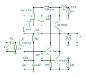
I’ve put my thread opening sim of Graham’s circuit together with my modded circuit in the following sim with a complex excitation, 3:1 2 and 20 KHz input at ~ ½ max swing let you look at intermod skirts as well as harmonics, a 1 A, 7 KHz current source in series with the speaker load shows output impedance and intermodulation interactions with the 7 KHz output disturbance that clearly show the advantage of increased gain
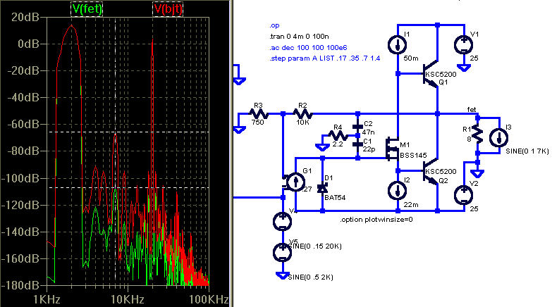
Increased loop gain at audio frequencies has improved 2 KHz harmonics ~ 30 dB and the 7 KHz output current induced signal is ~ 40 dB down with the mods in this sim
Speaker cable impedance will prevent the low level of the output impedance ( ~ 10 uOhms! ) from helping at the loudspeaker end but the amplifier’s distortion should show greater immunity to Graham’s “back EMF” concerns
How about some more gain?
Graham’s Class A Imagineering articles spend considerable space discussing amplifier output impedance and interaction with “back EMF” from the complex loudspeaker load, with the possibility of nonlinear back EMF components tossed in as well
Suspicion over feedback control of the output impedance with standard dominant pole miller compensation is suggested as a source of poor performance with the complex/nonlinear speaker load
Cherry has addressed the same issues in “Feedback Sensitivity and Stability of Audio Power Amplifiers” and “ Output Resistance and Intermodulation Distortion of Feedback Amplifiers” JAES V30 #5 May, April 1982
Cherry’s prescription is more gain, specifically more hfe in the VAS and more loop gain to address output stage current and voltage nonlinearities respectively
The JLH output stage Graham uses naturally provides voltage gain, borrowing another of Hood’s ideas (“Gain Stage Investigations” Electronics World july 1998) I changed the Q2 driver transistor (~= VAS transistor) to a small signal mosfet for increased “hfe” at audio frequencies
2-Pole compensation that includes the output stage is implemented with Graham’s component values, slightly rearranged, (Cherry’s nested feedback around the output stage)
I’ve put my thread opening sim of Graham’s circuit together with my modded circuit in the following sim with a complex excitation, 3:1 2 and 20 KHz input at ~ ½ max swing let you look at intermod skirts as well as harmonics, a 1 A, 7 KHz current source in series with the speaker load shows output impedance and intermodulation interactions with the 7 KHz output disturbance that clearly show the advantage of increased gain
Increased loop gain at audio frequencies has improved 2 KHz harmonics ~ 30 dB and the 7 KHz output current induced signal is ~ 40 dB down with the mods in this sim
Speaker cable impedance will prevent the low level of the output impedance ( ~ 10 uOhms! ) from helping at the loudspeaker end but the amplifier’s distortion should show greater immunity to Graham’s “back EMF” concerns
Attachments
Hi jcx,
I'm always on the lookout for a better performance from a JLH output stage, but in real life mosfets in general upset the resistor divided driver transistor pusp-pull output matching at higher frequencies. Gain/NFB is not everything.
As an aside, you would need a current sink/mirror to implement I2, unless the driver resistors are dropped to circa 33 ohms ?
My amplifier is also tested in real-life as well as sim'd driving virtual loudspeaker circuitry.
Where has the 22pF NFB capacitor // 10k gone ? This is essential in real life because it affects the 'quality' of the reproduced sound.
Cheers ......... Graham.
Graham I’m certainly just playing with ideas in simulation but I’m not sure about your reasoning about the mosfet driver affecting output transistor current division
As a modulated current sink the driver can only shunt some of the bootstrap biasing current, the difference must flow in the output transistor bases
Real driver transistor parasitic shunt paths that could upset output transistor base current division such as Cgs,gd or Ccb,be, base current are negligible at audio frequencies for reasonable small/medium power transistors
suitable small signal mosfets have ~ 50 pF Cgs, 30 pF Cds, <10 pF crss – the main difficulty is getting them in packages that can handle ~ 1 W, sot-223 is a possibility
My circuit uses ideal current sources to simplify the sim, translating the ideal sources to real hardware requires evaluation of the local loads,
in http://www.tcaas.btinternet.co.uk/jlhupdate.htm the author finds it desirable to use a active current source in place of the bootstrap
I’ve increased the drive transistor bias current guessing that reduced modulation of driver properties with ic(d) is worth some extra power dissipation and the possibility of needing another active current sink but the sim with the KSC5200 output transistor shows ~7.5 Ohm incremental base resistance so even a 36 Ohm current sink bias resistor only causes a 2 dB reduction in gain vs the ideal current sink
the 22 pF cap is now part of the compensation network applying feeback over an even shorter local loop around the output transistors - are you asserting that a ~ 1MHz pole is necessary for your "sound"
- Status
- This old topic is closed. If you want to reopen this topic, contact a moderator using the "Report Post" button.
- Home
- Amplifiers
- Solid State
- Graham's Class A/JLH output