An externally hosted image should be here but it was not working when we last tested it.
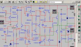
This was intended to be a simple general-purpose amp made with cheap industry standard components but trying to get the maximum performance of them. I decided to publish it just in case somebody finds it useful or interesting [unlikely to happen I think]
I plan to made dual bridgeable boards and use a couple of them to drive two midbass horns [15" 4ohm drivers] and also as a replacement for my current test amplifier that is not happy driving low impedance loads since it's based on TDA7294 ICs
The first prototype [LTP, VAS and VbeMult in bread-board, output stage point-to-point] showed marked parasitistic oscillations between 30 and 40 Mhz generated in the output stage [the amp has no global feedback at so high frequencies so the global loop can't oscillate]. This just proves that emitter followers can an do oscillate. I solved it by improving the [point-to-point] layout and adding 68pF and 22pF lag capacitors to the drivers
The amplifier loop itself has lots of feedback but in normal operation there are no signs of oscillation, only slight ringing when coming out of clipping. Predicted open loop gain is 104dB and there's still 100dB of gain at 10Khz. Closed loop gain in that schematic is 25dB [it may be reduced to 20dB] so there is 80dB feedback across most of the audio band. Feedback ends at about 3Mhz thanks to the 9dB/oct roll-off provided by the pole-zero compensation that bypasses the Vas buffer at HF and the Vas lag capacitor, instead of the classic 6dB/oct rolloff
It has good rail efficiency, clipping at 6A per device output current happens 2 volts below V+ and 1.5 volts above V-. Test rails are +-20V regulated, next step will be +-40V regulated rails [BC550C and 560C are actually BC546 and BC556 in the prototype]. Lower clipping was actually 1V below V- but I had to add a baker clamp in order to prevent oscillation caused by excessive output stage saturation when coming out of clipping [1N4148 is rated at 75V so I have to use higher voltage diodes to test +-40V rails]
It also features good thermal stability since the Vbe multiplier transistor is a low Vbe type and is operated at only 100uA Ic. This ensures lower Vbe and higher temperature coefficient on that transistor in comparison with the output devices, so there is some degree of negative thermal feedback. To understand how Vbe and temp.coef. are related with Ic see P2N2222A datasheet from On-Semi. I've tested it with up to 200mA of bias and it changes only about 15mA from 20ºC to 50ºC. In the past I've got allways unstable bias and thermal runaway with single transistor Vbe multipliers, particularly when they are operated at several mA Ic
That's all...

I've just tested it with 40V regulated rails and this has revealed some interesting things. Note I'm actually using a single pair of output devices and drivers in that prototype
TIP35C/36C and BD139/140 Vbe markedly decreases as Vce is increased, so 100mA of bias adjustment with +-20V rails translates to more 300mA of bias when +-40V rails are applied. I forgot to set the bias to the minimum before testing
Other transistors also suffered Vbe change due to Vce change, so I had trim the 600 ohm resistor of the Vas buffer to 520 ohms and the 220 ohm Rbe of the VAS also asked for a slight reduction in order to mantain the same buffer bias. Output offset was about 4mV
Testing with LF signal and 4ohm speaker load [Re=3.3ohm, horn loaded] revealed no oscillations in normal operation, but there was more than desirable 1 to 3Mhz ringing when entering and leaving clipping at both ends [global loop unstability], so I increased the 68pF Vas miller capacitor to 2x 68pF and oscillations disappeard
Rails were exactly +-40.6V and output swing was +38V and -39V for an estimated output peak current of 10A
Then, I decided to test it at full output swing with some degree of clipping [typical working conditions of most PA/disco amplifiers] and after a few minutes I got both TIP35C/36C with b-c-e shorts, BD140 driver with emitter open and b-c short, and BD139 driver with serious leakage altough not shorted
The BD140 devices I'm using are not-branded, probably fakes, so I suspect the BD140 driver was the first to fail, it probably has very poor SOA compared with the genuine device. BD139 units are also under suspect of being fakes, altough their marking starts by 'PH'
Blown TIP35C/36C were genuine devices as the die size was 4.5mm by 4.5mm on both. With 40V rails and 4ohm load with less than 30º inductive current lag they were clearly operating inside their DC SOA so they are unlikely to be the first devices to blow
Anyway, next step is to test the circuit with MJE15028/MJE15029 drivers to confirm that TIP35C/36C are not the cause of the problem, while I order genuine BD139/140 units. There are plenty of transistors suitable as drivers but the circuit requires its Ft to be >50Mhz to keep its high bandwidth
BD139/140 Ft ranges from 100Mhz to 200Mhz so the output stage appears essentially as a single pole-zero coming from the Ft=3Mhz of the output devices. In comparison, output stages made with old&cheap Ft=3Mhz drivers and Ft=3Mhz outputs show two superimposed pole-zeros, so output stage by itself reaches 180º lag around 3Mhz and requires lots of compensation to make a stable amplifier [with much lower bandwith]
Too much to see here Eva, interesting design
But, really will only show that, with no doubts, you are a very skilled person, a competent designer, and all that, and much more, we already now very well related your person, resulted the strong impressions you left with us.
I gonne to simulate, but spend more than one our, and this is my timing limit to simulate amplifiers....if delays too much, no good to home made, to diy applications in my personal idea.
Japanese factories are running to simple designs, as one i am sending, they are avoiding too many circuits and stages, and there are many reasons for that, we do not need to discuss here, because very well known.
I am, a long time, watching and following the "ligth" that came from you mind.... and waiting, with patience, the day you go to a simple design, to be honored with this gift to us.
I will be waiting.
regards,
Carlos
Attachments
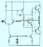
Famous Japanese factories are going this schematic.
The reasons are many, we can write a book, and together many Enciclopedias related this kind of circuit.
To hold your low impedance, have only to put a lot of pairs in parallel in the output.... can use cheap units, alike TIP41/42 or higher speed units too....many emitter resistors and ready to make shorts in output without problems.
I am studying hard this schematic.... discovering a lot of things, but i am not an enginneer and have not all the "instruments" you can have to calculate exactly the performance....I am going changing parts, listening, and trying modifications..... sometimes i am lucky, sometimes i loose my time.
This circuit can reproduce astounding bass, and incredible highs.... i could not put them together in the same amplifier... wainting some good "soul" to make this kind of design to have completely balanced related bass and treble.
A very famous Japanese Company, one of the biggest is doing, now a days, this circuit inside their chips..... only the voltage and some external resistors are changed, in hi power units, more output transistors are allowable.
And i am going showing this thopologie, till the day some enligthed mind decided to go deep, and in special, opens their results to us.... complete results, without some special conection hidden or ocasionally forgoten.
regards,
Carlos
Attachments
Eva,
How did increasing the miller cap affect your high frequency(audio) responce, as far as mis-shaping the sine wave toward a triangle waveform?
Also have you tried placing one of these small caps from the output of VAS to inverting input on the differential amp?--(looks like Q11) This may help the amp a little when driving capacitive loads; higher frequencies.
I like the idea of a negative temperature coefficient concerning the output stage & compensation. However if you can achive a temp. coefficent of ~1, then you could probably get away with less Ic bias through the outputs without the heat causing them to operate in cuttoff and have crossover noise.
Update :
Now I think that the output stage disaster was due to a bad connection in the wires that connect the Vbe multiplier [placed in a hole on the heatsink] to the breadboard. After replacing the blown transistors I found those wires intermitently losing contact, but luckily this time it happened while testing the circuit with +-20V rails from a regulated supply based on LM317/LM337 Ics that is not able to provide destructive currents
The circuit works properly with MJE15028/MJE15029 drivers but now I get more persistent 0.5 to 1.5Mhz oscillations when entering and leaving negative clipping, even with 2x 68pF Vas lag capacitors
Carlos : For +-20V rails use R21=1Kohm, R7=R8=330ohms 1Watt and D2 is no longer required. The component values shown on the original schematic were calculated for +-40V rails
cunningham : To check the actual open-loop linearity and general behavior of the circuit I'm monitorizing Ib of the Vas transistor through a 1K resistor placed between que collector of Q12 and ground. This current waveform contains both a component proportional to the input signal and a component proportional to the difference betwen the amplifier output voltage and the input voltage, so here I can 'see' in detail all the distortion the circuit actually introduces and the LTP is trying to correct [example : the infamous switching spikes associated with too low quiescent current on te output transistors]
I've tested the circuit with +-20V rails driving 2.6 ohms resistive load at 10Khz at full power [about 36Vpp, 62Wrms] and there were no traces of triangle waves. Actually, the amplitude of the Vas buffer Ic waveform while providing full power into 2.6 ohms at 10Khz was only about 20% higher compared with the amplitude with no load, and it was pretty sinusoidal [with little class AB switching glitches] so I think it could be said this amplifier is almost 'load invariant'. The output stage driving 2.6 ohms at 10Khz still shows somewhat higher impedance than the 68pF capacitors, so capacitors dominate
I also tested it with +-40V rails driving 3.4 ohm resistive load at full power [about 76Vpp, 212Wrms] and the waverform was also very sinusoidal [ie : there is very little open loop distortion to correct by the feedback mechanism] even at this 'low' frequency where the 68pF capacitors no longer dominate. I have to repeat that test with +-40V rails and 3.4 ohm load but at 10Khz
About thermal stability, my last measurements show that the feedback is only negative for +-20V supplies. For +-40V the circuit is slightly thermally undercompensated. This happens because TIP35C/36C are very hard to compensate devices since its Vbe is around 500mV [it decreases for higher Vce] and 0.1 ohm emitter resistors also make compensation harder altough they provide very good rail efficiency
Reducing VbeMult temperature coefficient is very easy, I just have to reduce the value of the 22K resistor placed between base and emitter of the VbeMult buffer to increase Ic of P2N2222A and thus increase its Vbe and reduce its thermal coefficient. In the other hand, I see increasing the temperature coefficient of the VbeMult as a very complex task, maybe using a power device with even lower Vbe as a sense element instead of a P2N2222A?
While measuring different transistors in order to select a VbeMult sense element I got this data, and I think it could be useful for other people :
Device - Ic=110uA - Ic=30mA
BC550B - 570mV - 726mV
BC639 - 563mV - 692mV
PH2222A - 560mV - 690mV
BD139 - 547mV - 690mV
BD237 - 510mV - 651mV
TIP41C - 496mV - 638mV
BD911 - 425mV - 576mV
BD681 - n/a - 1223mV
TIP122 - n/a - 1168mV
Measured at Vce=2.1V and about 20ºC temperature
I forgot to mention that I'm using 0.1ohm 4W cheap ceramic wirewound resistors that are somewhat inductive and I had to bypass them with 2.2ohm standard 1/4W resistors to fully supress the 20..40Mhz oscillations I got at first on the output stage
I've also noted a very interesting phenomena related to bias stability : If I measure the bias inmediately after the amplifier was playing at medium to high levels I get a bias current value 2 to 4 times higher than the value I previously adjusted when the circuit was idle. Even more interesting : This unexpectedly high bias current quicly drops to the previously adjusted value in a period of about 10 seconds. Obviously this behavior is caused by the temperature drop across the thermal resistance from the dies of the output devices to their cases and to the heatsink, that may reach 10ºC or more while playing [output devices are dissipating nearly 120W peak]
Suggerences to minimize or prevent this phenomena are welcomed. Currently I'm using a steady state bias current 3 times lower to compensate for the temperature difference [I set 15mA idle bias to account for 40-60mA while playing]. I have no distortion analyzer so I adjust the bias to minimize the switching spikes seen on the Ic of the Vas buffer. Altough the best waveform shape at 10Khz is obtained with 500mA to 1A bias!!!, a more practical value like 50mA is enough to fully supress switching spikes and get a nice looking waveform at 1Khz but with a couple of glitches at 10Khz
Finally, I wonder why there are so much posts related with amplifier simulation but there are so little posts related to comparing simulation results and waveforms to real results and waveforms measured on actual circuits. Simulation is extremely useful but I think there is no point in finetuning simulation circuits, this is only useful for real prototypes
Rigth, i saw Japanese doing that!
I saw they hearding for long time, many japaneses from various factories departments.
And they made notes related subjective feelings.
When finished the hearing tests, they gonne to instruments, to increase their habilities to understand what each waveform shape means to audio perception.
You are completely rigth in my idea... direct in the target!
regards,
Carlos
Eva said:Update :
Reducing VbeMult temperature coefficient is very easy, I just have to reduce the value of the 22K resistor placed between base and emitter of the VbeMult buffer to increase Ic of P2N2222A and thus increase its Vbe and reduce its thermal coefficient. In the other hand, I see increasing the temperature coefficient of the VbeMult as a very complex task, maybe using a power device with even lower Vbe as a sense element instead of a P2N2222A?
I've also noted a very interesting phenomena related to bias stability : If I measure the bias inmediately after the amplifier was playing at medium to high levels I get a bias current value 2 to 4 times higher than the value I previously adjusted when the circuit was idle. Even more interesting : This unexpectedly high bias current quicly drops to the previously adjusted value in a period of about 10 seconds. Obviously this behavior is caused by the temperature drop across the thermal resistance from the dies of the output devices to their cases and to the heatsink, that may reach 10ºC or more while playing [output devices are dissipating nearly 120W peak]
Suggerences to minimize or prevent this phenomena are welcomed. Currently I'm using a steady state bias current 3 times lower to compensate for the temperature difference [I set 15mA idle bias to account for 40-60mA while playing]. I have no distortion analyzer so I adjust the bias to minimize the switching spikes seen on the Ic of the Vas buffer. Altough the best waveform shape at 10Khz is obtained with 500mA to 1A bias!!!, a more practical value like 50mA is enough to fully supress switching spikes and get a nice looking waveform at 1Khz but with a couple of glitches at 10Khz
I just noticed the feedback pair Q14 & Q15, used as the servo for thermal compensation. This is interesting, usually the servo transistor is chosen to have similar charactoristics to the output devices. Temperature coefficient is related to Beta.
As for your glitches at higher frequency, increasing the gain of your differential may help some. Try using a current source\mirror to bias the collectors of Q10 & Q11.
I have delt somewhat with what you are saying about the output bias being large due to the internal instantanious temperature. This could be a problem because the NPN gets hot when the signal is positive, and when the signal goes negative, the NPN bias is still to large. When considering the DC load line of class AB biased power devices, this could create a current spike as DC current flows through the NPN into the PNP(which is on) generating unwanted heat and vice versa.
If you can cause the NPN to be compleatly turned off when the signal is negative instead of continuously having NPN bias on then this may add some stability to the DC load for the outputs and also better thermal stability. With 40mA bias the NPN has to dissapate like 3W when the signal is -30V.
Suggestion: Try replacing R5 with two series diodes, like small 1A diodes, forward bias. The small power diodes will have a larger forward bias than Vbe, or what takes to turn on the outputs so servo adjustment, R31, will still be able to set bias and it will be more stable, particularly setting a maximum bias on the outputs and less chance of melting them with poor bias adjustments. Not saying yours is poor, I just don't like having to buy new outputs. As the signal goes negative, the internal resistance between base and emitter will have a larger voltage drop relative to instantanious current output; Vbe will increase as the PNP output is driving a load. This means that the base voltage on the PNP will be lower than the emitter voltage and, through the two diodes, pull the base of the NPN down more with it causing the NPN output to cuttoff, because the NPN emitter is same potential as PNP emitter.(relatively) As the signal aproaches crossover, the NPN will turn back on with bias current.
Anyway...good day
tee z rah oh n
Do not know if this is your question or not...but, if the question is that one:
What is the software you used to make some image from a commercial circuit.
The answer is Multisim 2001... Eva is using other one, i do not remember the name...ask Eva.
Related Eva, she is showing her own design...no problems....
Related Me, Carlos, i am showing a Comercial Japanese design, this way had to copy in a simulator and make some differences to avoid copyrigth problems...not a copy... some adaptations made it loose this characteristics...not more the one, also cannot be a "clone"....is only "alike"... similar....not the one!
Carlos
I will return to this schematic near future...now it is resting
Gave me some work, and create some problems too...boooom!
This way, i will return in near future.... with the 100 ohms protection resistor it smoked... my mistake probably.....this is not uncommon.
regards,
Carlos
Gave me some work, and create some problems too...boooom!
This way, i will return in near future.... with the 100 ohms protection resistor it smoked... my mistake probably.....this is not uncommon.
regards,
Carlos
Update [the last, I think] :
Blown devices were definitely due to false contacts in the Vbe wires. I rebuilt the output stage again with no-band BD139/BD140 and succesfully tested the circuit with a single pair of output devices [and drivers] at full power at 10Khz for some time, and also as a mid-bass amplifier driving a horn-loaded 15" with music signals at full power for hours
A current mirror was added to provide low offset [2mV with randomly selected transistors] without having to trim anything. A current source was not added since the 120K resistor already provides a current-source effect to the LTP. To compensate for the 6dB extra open-loop gain introduced by the current mirror I had to add 100 ohm emitter resistors to the LTP to reduce open-loop gain
The bridge input was removed since I'm planning to add a dual op-amp using the -15V supply from the Vas and an extra +15V supply generated with other zener to provide differential inputs. An output inductor was added since it appeared to improve phase margin
The capacitor between the bases of the output devices was removed since measured changes in cross conduction at audio frequencies with it and without it were very small, and the capacitor caused trouble when clipping
Clamping diodes were added to prevent hard saturation of the output devices, providing no ringing at all when recovering from hard clipping of a 10Khz sine wave and still +-37.5V swing into 2 ohms with +-40V regulated rails [350Wrms@2 ohms with two pairs of output devices, 700Wrms bridged into 4 ohms]
An externally hosted image should be here but it was not working when we last tested it.
Blown devices were definitely due to false contacts in the Vbe wires. I rebuilt the output stage again with no-band BD139/BD140 and succesfully tested the circuit with a single pair of output devices [and drivers] at full power at 10Khz for some time, and also as a mid-bass amplifier driving a horn-loaded 15" with music signals at full power for hours
A current mirror was added to provide low offset [2mV with randomly selected transistors] without having to trim anything. A current source was not added since the 120K resistor already provides a current-source effect to the LTP. To compensate for the 6dB extra open-loop gain introduced by the current mirror I had to add 100 ohm emitter resistors to the LTP to reduce open-loop gain
The bridge input was removed since I'm planning to add a dual op-amp using the -15V supply from the Vas and an extra +15V supply generated with other zener to provide differential inputs. An output inductor was added since it appeared to improve phase margin
The capacitor between the bases of the output devices was removed since measured changes in cross conduction at audio frequencies with it and without it were very small, and the capacitor caused trouble when clipping
Clamping diodes were added to prevent hard saturation of the output devices, providing no ringing at all when recovering from hard clipping of a 10Khz sine wave and still +-37.5V swing into 2 ohms with +-40V regulated rails [350Wrms@2 ohms with two pairs of output devices, 700Wrms bridged into 4 ohms]
Eva said:Update [the last, I think] :
The bridge input was removed since I'm planning to add a dual op-amp using the -15V supply from the Vas and an extra +15V supply generated with other zener to provide differential inputs.
]
I am a fan of OP-AMPs but if I can get away with not using them in the signal path, tis better off. If constructing a circuit is not too much effort for you, I would use another differential circuit & VAS for the input, then you have an inverting and a noninverting input. Design the circuit so the overall gain is around 1 or so. More complicated, but better results
- Status
- This old topic is closed. If you want to reopen this topic, contact a moderator using the "Report Post" button.
- Home
- Amplifiers
- Solid State
- My new amp [not much to see here]