Nelson Pass said:That looks like finished product compared to my
prototypes.
Hmm, are you using free-air wiring ?
Mike
I barely even use any wire for mine since if I could clip all leads to nothing and butt components up to each other I would. I never get time to make PC's since the circuits go through continual evolution, with more things to try than I ever have time to get to doing. I am not too incilned to show off any of my asseblies which may be one reason why I don't have a camera. I have been seeing some good pictures here.")
MikeB said:Hmm, are you using free-air wiring ?
I construct in 4 dimensions.
I have three stages of prototyping, although depending on the complexity of the circuit I usually don't need all three.
1) Breadboard. Great for chucking together circuits quickly, but not suitable for circuits where physical layout is important.
2) Stripboard. More permanent than breadboard and with more layout freedom.
3) Full prototype. Made as if it were the finished article. Only small changes made from here. Good for shaking out grounding problems and other things that are difficult to simulate.
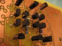
Here's a pic of a 3): http://www.cheese83.freeserve.co.uk/amp/amp3/prototype.jpg
1) Breadboard. Great for chucking together circuits quickly, but not suitable for circuits where physical layout is important.
2) Stripboard. More permanent than breadboard and with more layout freedom.
3) Full prototype. Made as if it were the finished article. Only small changes made from here. Good for shaking out grounding problems and other things that are difficult to simulate.
Here's a pic of a 3): http://www.cheese83.freeserve.co.uk/amp/amp3/prototype.jpg
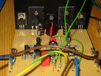
Here is my prototype of the Holton's AV400
Right now i'm waiting to local metal workshop building the case for this amp.
- Naula
Right now i'm waiting to local metal workshop building the case for this amp.
- Naula
My prototype project work list:
0) Idea
1) Simulation of concept
2) Bread board – pick components so you know their housing and pinout (important for debugging)
3) Simulation and debugging of real world circuit.
4) First PCB made as simple as possible to verify all footprints and pinouts
5) Simulation of corrections that need to be made – any new components?
6) Final PCB
I have found that it’s possible to make 2 layer PCB’s relatively easily. Just remember that any connections between the two layers need to be easily accessible. I often use resistor pins because they are easy to solder on both sides of the PCB.
Avoid connections between the layers by means of boxed capacitor pins, as these are difficult to solder on both sides.
\Jens
naula said:Here is my prototype of the Holton's AV400
Right now i'm waiting to local metal workshop building the case for this amp.
- Naula
Which metal workshop company do you use
I've been using par-metal but the custom import chanrges are killing my pocket
My is pretty close to Jens.
1. Idea as Jens wrote
2. Simulation too
3. Check for available parts.
4. Read the datasheets one more time.
5. Put the parts into the cad system and check their dimensions.
6. Make schematic
7. Make the PCB layout
8. Check the schematic one more time.
9. Check the PCB layout
10. Send the gerber files too www.elprint.dk
11. Build one unit and ttest it through..
Yes i know there is no steps in between where you see a prototype board..
Only if it is something i cannot find a topic on or does not understand i will make a breadboard.
But i have come that far that i can go from sim to finished product the most of the time. It take some preparation but it will pay of.
naula said:Here is my prototype of the Holton's AV400
Right now i'm waiting to local metal workshop building the case for this amp.
- Naula
Hey, i understand the functions of most of your parts, but what is
the toaster good for ?
Mike
My steps are:
1, have an idea
2, simulate (maybe discard, and back to 1)
3, have a look into my box, and check available parts
4, change ckt for available parts and simulate again
5, heat up the soldering iron (or how is it called ?)
6, put together the ckt, typically takes 1 or 2 evenings
7, test
8, clean up the table from banged devices
9, listen
10, modify and simulate
11, put it into the other box...
Mike
mskeete said:
Which metal workshop company do you use
I've been using par-metal but the custom import chanrges are killing my pocket
The Finnish name of this workshop is TK-metalli. I don't know much more about the company. Estimated price of the case is 50 - 100 EUR. Not so cheap but the case is always the hard part.
MikeB said:
Hey, i understand the functions of most of your parts, but what is
the toaster good for ?
Mike
Maybe I will use the toaster by resistive load for the amp and toast a toast with test signal by Tshaikovski
Or would it be better taste with pure sine wave?- Status
- This old topic is closed. If you want to reopen this topic, contact a moderator using the "Report Post" button.
- Home
- Amplifiers
- Solid State
- Prototypes...