Appreciate shared knowledge and test data or pictures from experienced amplifier PCB designers. Thanks...
Design target: 25-50 watt Class A low voltage, high current amplifier with 4+4 output transistors
What the best PCB layout?
1) A single PCB that takes advantage of high capacitance density of 10-16V caps.(attached)
a) create a star ground point on PCB
b) attach rectifier diodes above PCB star ground point with short copper bus bar
b) put input adjacent to PCB star ground. Put output close to input for short feedback path
c) many small caps on PCB for unregulated output power supplies. 0.3-0.5F total
d) modest power regulated supplies for driver circuitry on PCB
e) use 1" stand-offs to mount PCB to heatsink to reduce heat transfer
2) Two PCBs wired together
a) PCB for output transistors and output power supply filter caps mounted to heat sink
b) PCB for driver circuitry and regulated power supply
c) wire both boards to star ground point at rectifier diodes
d) wire feedback directly from output point to feedback point on driver PCB
3) Better alternative?...description...data...picture?
Attachments
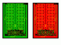
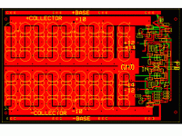
The example PCB layout is ~ 60 sq inches...9" x 6.6", $23 prototype quantities 2 layer, 2 oz copper.
Four output transistors are evenly spaced on each 9" edge, eight total, attached to the heat sink. 48 x 8,200uF @16V capacitors are on the PCB for the +/- 10V unregulated output power supply.
Four output transistors are evenly spaced on each 9" edge, eight total, attached to the heat sink. 48 x 8,200uF @16V capacitors are on the PCB for the +/- 10V unregulated output power supply.
What the best PCB layout?
I think this book has a section on pcb layout recommendations.
http://www.amazon.com/exec/obidos/t...f=sr_1_1/002-8841616-0527253?v=glance&s=books
1 vs 2
From what I've noticed, most people here chose to make
the pcb's small to reduce cost, that seems to be #1 priority.
I did a layout of a 6.5" x 10.75" board, 4 layer and it cost alot.
qty 10 @ $1000.00
qty 20 @ $1200.00
+$250 NRE
Well, I don't know. If your total PCB area is the same, I'm pretty sure a single one would be cheaper than two parts, unless it gets so big that the manufacturer has to use special machines. That will rarely be the case in audio.
Your board is 1) pretty big, and 2) 4-layer. That's not your regular audio PCB, and the 4 layers really up the price.
Jan Didden
Your board is 1) pretty big, and 2) 4-layer. That's not your regular audio PCB, and the 4 layers really up the price.
Jan Didden
I can attest to two considerations that the origan poster inquired about.
Location of output relative to input -- keep them away from each other. An otherwise stable amp can become an oscillator just by putting the output circuitry in close proximity to the input! In fact, I'm moving toword the idea the best place for the zobel and output inductor (if you use them) is off the PCB and at the binding posts.
Power ground and signal ground (signal return?) should be separate and exit the PCB from different points. This implies the star point is off-board. There may be some ambiguities with some ground points as to whether they are power or signal related. I use the rule that if the purpose is to provide a low impedance path for unwanted signals "riding the rails", its a power ground. Treating the zobel as above moots what to do with that.
Challenges of a small board amp
I have always used smaller PCB's but not for cost. The benifits are short paths low inductances and and low stray caps to degrade performance. However the big challenge is keeping the magnetic fields at bay. There is a lot of current in the output section and it will couple into an trace parallel even if the trace is some distance away (by PCB standards). The biggest offenders are the leads around rectifiers and filter caps. Since these are dealing with line frequency the noise induced has nothing to do with audio and is very audible.
What I did in the Spectral amps was move the low level circuits into a small daugter board at right angle to the main board and orient it as best possible at right angle to the main current path.
I always kept the rectifiers and main supply caps away from the board. Smaller local caps (1000 uF) handled the HF currents and the remote (10" of #12 wire) 50,000 uF caps dealt with the high current low frequency requirements. It also kept the rectifier close to the transformer, reducing the radiating window in the supply leads.
I prefer bridge tied loads as the best way to keep unwanted currents out of the ground, however it greatly increases the complexity of the amp.
Ohter people have different philosophies here but these have always worked well for me.
Demian
Spectral was one of my favored firms, 'cos was made very high speed amps, which I like too and had clear and logical prospect. But explain me, why this firm recomend for his product cables, which absolutely kills good parameters of this amps, 'cos this cables have inside high cut filters, which cut hearable in acoustic band ? Is it not somewhat contrast demand ? Or aren't this amps stable ? Or is it for, that here exist close relatives between both owners, how I heard somewhere ?
Upupa Epops:
The problem with wideband stuff is keeping it stable. The amps have a power bandwidth of 500KHz opening new vistas of problems to solve. When we introduced it there were some pretty strange cables and we found the best solution to the problem was to supply the cables that worked. This was a good business decision and solved the intermittant stability problems. The amps have improved in their stability (we have all learned a lot) and are more cable tolerant, but the business side seems to still think its necessary to stay with the program.
sam9:
I used a Berg connector pair, very like the Molex connectors, two rows of pins on .1" centers. We paralleled pins for reliability and it worked pretty well. We also had mecanical connections to keep the boards tied together.
-Demian
my experiments over the years suggest to me also to move these components as close to the output posts as possible.
i think i read in the Leach amp papers he prefer this also.
i think i read in the Leach amp papers he prefer this also.
sam9 said:... In fact, I'm moving toword the idea the best place for the zobel and output inductor (if you use them) is off the PCB and at the binding posts.
WOULD REMOVING THE OUTPUTS BE ENOUGH?
Thanks for sharing your experiences.
Would removing the output traces from this one PCB be a good solution? The bipolar emitter outputs could be star wired, and a feedback wire attached to the differential amplifier on this PCB.
Would it still be better to put the low level driver circuit on a separate PCB in addition to removing the high current AC outputs??
Attachments
A few more reactions to your drawing:
1) If the outputs are bipolar I think you need more driver heatsink if not a bigger driver.
2) look at the loop the currents will take from the supply rails to the load and back. If they wrap around the input circuit or the feedback lines from the output they can generate errors and unintended feedback. I didn't see the emitter resistors on the drawing so I'm not sure how you will handle those issues.
3) I would keep the output circuit on the board with large traces and use your interdigitated layout with the outputs included. Either move the driver circuit to a seperate PCB or set up a shield between them and the input section. You could use two shields- one tied to ground over the input circuit and a second, tied to the output seperating the voltage output from the ground- it will reduce the capacitance that the voltage section drives.
What kind of bandwidth and max current were you planning?
-Demian
1audio said:What kind of bandwidth and max current were you planning?
-Demian [/B]
6 amps Class A into 1 ohm load, flat to 128KHz
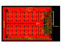
I've attached a PCB sketch that puts the input on one side with the low level circuitry, and the output at the other end. A wire is necessary to connect the output to the feedback path at the intput differential stage. From the discussion, it seems that a layout like this might be the best possible for one single PCB.
Any other suggestions?
Attachments
The layout looks good. Here are some notes based on my experiences-
6 A into 1 Ohm or 36 W RMS. In class A that would mean about 75W dissapation. Watch the thermals since the power capacity of the transistors goes down fast as they heat up.
The driver should be able to deliver 600 mA to the bases of the output transistors or more. The Beta falls with frequency so the drive requirement increases.
The current requirements actually suggest using fewer transistors. You will be in a more linear range and 10A PK at 150 KHz is not a difficult requirement for a single transistor. I would use the latest Power FET's but thats what I am comfortable using.
After a little other looking I have determined that this is for direct drive of a ribbon. I did that 25 years ago. It does work well. I would make the following suggestions based on my experience (including making a diaphragm for a Decca the evening before a CES opening when the amp cooked the working one).
1) Cap couple the output. No need for a servo with the cap and the worst case offset should not matter.
2) Use a relay across the speaker terminals until the amp settles. The charging of the cap will kick the ribbon out of the gap.
3) Use a current amplifier. The ribbon responds to the current, not the voltage. The resonance of the ribbon is very low frequency and low Q so damping is not an issue. It will compensate for inductance and resistance in the connections (and for the coupling cap).
4) The ESR and self inductance of the coupling cap will become critical since it will be a large part of the series Z. Look for a way to move it out of the intended frequency band.
If you need to measure it I am not far from you and have all the stuff to measure almost any aspect of the amp or the driver.
-Demian
- Status
- This old topic is closed. If you want to reopen this topic, contact a moderator using the "Report Post" button.
- Home
- Amplifiers
- Solid State
- best amp PCB layout..1 vs 2 PCBs