As far as a gain just larger than one, I can't help you. Otherwise, I would suggest a current source loaded source follower (2 FETs), which would have a gain just slightly less than one. Two pieces of 2SK170 (low current drive) or PN4293 (high current drive) would do the trick. The line amp I'm currently playing with has a common source stage with source degeneration, followed by a current source loaded source follower. Overall gain is 14. Harmonic distprtion is flat at 0.4% from 20-20k, and the distortion is overwhelmingly 2nd harmonic. I intend to put this line amp directly behing a 10k ganged cermet linear potentiometer with suitable shunt resistor to have it approximate an audio taper pot.
JFET ok?
http://www.till.com/articles/GuitarPreamp/
You didn't say no output capacitor although I suspect if you don't want an input cap, you might not want an output cap which would make this design process significantly more challenging...
--
Danny
http://www.till.com/articles/GuitarPreamp/
You didn't say no output capacitor although I suspect if you don't want an input cap, you might not want an output cap which would make this design process significantly more challenging...
--
Danny
Here's something I just put together in Orcad. You'll probably want to tweak it yourself though. No "signal" caps, the gate and drain are direct coupled to ground. The bias drain resistor is pretty touchy though. The source resistor sets the standing current to around 5mA. The main tradeoff is with the sizing, both drain and source resistors can be scaled somewhat, by making them larger it'll make the bias easier to finetune but you sacrifice damping factor. If you actually try it let me know, I just did it in simulation to see if it would work.
--
Danny
--
Danny
Single FET
hi all, Tks for both advises.
1. I will to build a single FET version first, ten try the current source to see how it can efect the sound. wrenchone can you kindly provide the diagram and FET selection process?
2, For the MOSTFET amp which device do you use, Azira? I have only twice done the FET pre, and recently mostly with tubes. So my knowledge about JFET is not good not to mention MOSFET. But the circuit look very interesting.
I hope to a JFET amp just as a utility amp, which I can use as a small and convinient pre that I can even carry around. the output cap is the price I am willing to pay, and I have lot of good cap in my parts boxes.
The MOSFET is interesting experiment that can teach me on the device...
Tks again and best rgds
William Lee
If you knowledge is limited and you're looking to learn, I suggest that you don't tie both hands and a foot behind your back by disregarding signal caps. The reason for this is that your loading becomes a factor in your dc biasing. You would be best to try building the JFET line stage, it fits your requirements and is a proven design.
The MOSFET in my circuit can be anything, it's not important, I think I might have picked an IRFP240. That's a power FET and you don't want a power FET so a different device might do much better, perhaps a small signal fet with higher transconductance. I really do not recommend building that circuit unless you can analyze it, it is very likely not to work as is. It was more of an answer to the challenge "can a single stage FET design be direct coupled on input and output?" It seems the answer is yes.
Good luck!
--
Danny
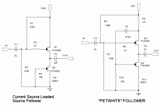
Here are a couple of circuits that cheat and use two JFETs, though you could substitute a source resistor for the bottom FET in the circuit on the left and get away with it, though most likely with higher distortion. The circuit on the right uses feedback from the top FET's drain to mudulate the bottom FET - sort of a Scottman's push-pull. It is similar to the White follower tube circuit. You will of cource need bypass caps on the 30V supply - the type and value will depend on the regulator you use to ge the 30V.
Attachments
Tks and any gain...
Tks again to both of you. The MOSFET line stage looked interesting except will it be stable as far as DC offset is concerned? I think I will try teh single FET line stage first. I have J 202. But the last time I try I could not get any gain above 1.... I was using similar circuitry.
I have just bought some 2SK type, I think 2SK 170 and 389 bi-Fet, will take a look what I have got.
Tks again and best rgds
William Lee
If you are using a common source stage as a line amplifer, you have 1) an inverting stage 2) not necessarily a low output impedance 3) can have difficulty getting a large symmetrical output voltage swing with a gain near unity, depending on your VCC and quiescent operating current. If all you are trying to do is to buffer your input sources, a source follower of some sort may be the best choice, even though the gain may be a little less than unity. With the source follower, you can have a reasonable output voltage swing and a low output impedance, with no phase inversion.
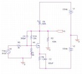
For the line stage I'm developing for my new preamp, I wanted some voltage gain so that I could compensate for a possible weak signal source. I also wanted the amplifier quiescent point to be at 1/2 Vcc for maximum possible signal swing. Some juggling with PSpice led to a stage with a gain of 14. This was a little higher than I wanted, but no big deal, since this stage will follow a volume control. What I ended up with was a common source amplifier with source degeneration feeding a source follower with current source loading. I used the "FETWhite" output circuit to get a little more output drive capability. It measures very nicely, and will be paired with a discrete JFET open loop RIAA amp built around a similar gain block. I'll have to wait until I can get the whole mess into a box before I can hear it. It will be interesting so see if I can notice any effect from the phase inversion.
I used the PN4393 devices for the line amplifier because thay are relatively low noise, have a high breakdown voltage (40V), and also can be selected for high Idss for good output current capability. They are also medium gain devices, so they don't require as much degeneration to trim the gain to the desired value. They are also easy to find. I am currently using matched output devices(within 0.1 ma Idss) selected for about 22-23ma Idss. Idss matching seems to be sufficient for decent results in this application. Output stage quiescent current is about 8ma. If you were fussy, you could set up an 8ma current source (or whatever other reasonable quiescent current you choose) and select devices based on the Vgs at this operating current. This will work even better. I used the simpler method because I had just moved and couldn't find my FET matching jig... The input device was selected to properly set the quiescent operating point, and if I remember correctly, was around 11ma Idss.
J202s have a pretty low Idss range and relatively low gain, and won't supply a lot of drive current. A better choice would be the PN4393 or 2SK170V, if you can find them. The RIAA amp used 2SK170 input devices, with a PN4393 output stage.
hi Wrenchone,
No Wonder my simple FET amp yield less then unity gain with common source ( that is output from the Drain?), it used 9 Volts B+, with the no matter how I arrange the ratio of the 2 RDrain and RSource!
On hand I have K240 bi-Fet, K 130, K373, and K 136. Actually I bought 2 each of all the FET i could find in the electronics supply shop I sed to go. Could you advise which one will be good for line stage and which for RIAA??
I think I have downloaded the spec for most of them except can't find the Pin out for the K240, could you advise the convention?
I roughly remember measuring the IDSS is to connect the Gate and the source together and pass, with R drain and apply B+ to measure the current flow, is that correct?
Also, is it ok to use no input resistor as in the tube amp if I were to have teh gate at zero volt?
tks again and best rgds
William Lee
Before you proceed you may want to read up on the matter. These are two excellent articles:
http://www.borbelyaudio.com/ae599bor.pdf
http://www.borbelyaudio.com/ae699bor.pdf
http://www.borbelyaudio.com/ae599bor.pdf
http://www.borbelyaudio.com/ae699bor.pdf
The two Boberly articles are a good though cursory introduction to using JFETs in audio circuits. The Siliconix JFET book is quite exhaustive, but it hammers at the math . If you can, get some more of the 2SK240s. They are probably your best bet for what you have in mind, unless you can find some 2SK170 or 2SK389 BL or V IDSS ranking. Look at the top of your K240s to determine the IDSS ranking. GR is 2.6-6.5 ma, BL is 6-12 ma, and V is 10-20ma. If you look at the flat side of one of the 2SK240 FETs inside its aluminum holder, the pinout is 1-drain, 2-gate, 3-source. Singapore must be full of electronics shops - you should be able to find anything you need. If you were in Hong Kong, I would tell you to go to Apilu Street.
- Status
- This old topic is closed. If you want to reopen this topic, contact a moderator using the "Report Post" button.
- Home
- Amplifiers
- Solid State
- Single FET line stage