tschrama said:Hi,
Sorry I didn't read the entire thread.. I now get your point. You're right about the input impedance. Bootstraping the input is a neat idea! In my arangement you can easely multipy all resistance values with 5x or 10x and re-adjust for mid-point voltage 20V... I actualy think you can leave those resistors out at the output pair.. the 2N3055 draws about 15-25mA basecurrent as it is.. this all has to be controlled by the little drivers... maybe indeed use a medium power transy there...
regards,
Thijs
No need to apologize, this is a very good discussion.
")
I wonder whether one could combine the bootstrap bias and collector feedback.
I ran some sims without the resistors on the drivers and I agree that at 40V they are likely not needed. I was thinking of something like the old TIP32 for the driver but I am going to look for a device with a little higher beta if possible.
I sim'ed your latest circuit and with a little bit of adjustment of the bias resistors (to center the DC voltage at the output) I was able to get results similar to my input stage. As I have said I don't think that the FFT results from my sims are very helpful as they don't seem to change much as I change the feedback arrangements but it looks like the emitter resistor feedback may give a slightly better distortion spectrum. The FFT shows slightly lower overall distortion with collector v.s. emitter feedback but the reduction is entirely 2nd harmonic with possibly even a slight increase in 3rd harmonic. In both cases the full output 2nd and 3rd harmonic distortion each varies from 35 to 45 dB down. What are your thoughts on the relative merits of collector feedback v.s. emitter feedback?
What I am looking at now is to see what will happen if I combine collector feedback and emitter feedback. I wil try adding emitter resistance to your circuit (and lowering series input resistance). I also want to play around with using less series input resistance with lower collector feedback resistance to see how that affects the FFT. It seems like the series input resistance throws out a lot of the input signal and it seems like lower closed loop gain and less signal drop would be beneficial.
Your thoughts?
Hi,
I use circuitmaker2000 for my simulations, and my experience is that it actually predicts the THD pretty good, compared with real measurements. I run 50 sinus cycles at 500 sample per cycle (AMD Athlon 2700+) , 1Watt in 8 Ohm at 1 KHz. It's importand that you use enough sample per cycle, else the sample rate ceils the THD.
If I run emmitor degeneration I get slightly worse THD , about +12dB comparitive to Collector feedback. Bootstrapping the input betters this by 6 dB. The collector feedback topology might benefit from the fact that is has a lower collector impedance to drive the output stage (about 1/5th) . However, it might have slightly less bandwidth compared to emmitor degeneration. Then again, collector feedback might have better Vsupply rimple rejection. It also has slightly more maximum voltage output, because no voltage is lost in the emmitor resistor.
It is still possible to use bootstrapping the collector load, but it doesn't help much; something which I don't understand. At 1 watt it seems that the input stage is dictating the THD, not the output stage; another thing that suprises me!
I don't think I completely understand your remark? In the collector feedback/series resistor topology the transistor-base is a virtual ground, but current is driving the transitor. In the emmitor feedback topology, a voltage swing at the transistor base is needed.
Cheers,
Thijs
I use circuitmaker2000 for my simulations, and my experience is that it actually predicts the THD pretty good, compared with real measurements. I run 50 sinus cycles at 500 sample per cycle (AMD Athlon 2700+) , 1Watt in 8 Ohm at 1 KHz. It's importand that you use enough sample per cycle, else the sample rate ceils the THD.
If I run emmitor degeneration I get slightly worse THD , about +12dB comparitive to Collector feedback. Bootstrapping the input betters this by 6 dB. The collector feedback topology might benefit from the fact that is has a lower collector impedance to drive the output stage (about 1/5th) . However, it might have slightly less bandwidth compared to emmitor degeneration. Then again, collector feedback might have better Vsupply rimple rejection. It also has slightly more maximum voltage output, because no voltage is lost in the emmitor resistor.
It is still possible to use bootstrapping the collector load, but it doesn't help much; something which I don't understand. At 1 watt it seems that the input stage is dictating the THD, not the output stage; another thing that suprises me!
It seems like the series input resistance throws out a lot of the input signal and it seems like lower closed loop gain and less signal drop would be beneficial.
I don't think I completely understand your remark? In the collector feedback/series resistor topology the transistor-base is a virtual ground, but current is driving the transitor. In the emmitor feedback topology, a voltage swing at the transistor base is needed.
Cheers,
Thijs
I don't think I completely understand your remark? In the collector feedback/series resistor topology the transistor-base is a virtual ground, but current is driving the transitor. In the emmitor feedback topology, a voltage swing at the transistor base is needed.
What I meant was that the series input resistor and the base-emitter junction impedence forms a voltage divider which drops most of the signal voltage across the input resistor rather than the transistor. What I think you are saying is that the input resistor and grounded emitter turns the circuit into a current driven circuit. Is that correct?
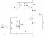
And now for something completely different. What do you think of this circuit. In my sims it seems to give the best results overall though I wish I could get the 3rd harmonic down some more. I have to run to work now so I haven't the time to check all of the currents. I would be interested in what this circuit does in your simulator. Note I am still using the small signal PNPs in the output because I don't have a model for a power PNP handy.
Attachments
Hi,
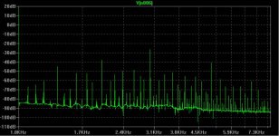
that's a nice update... I get -52dB where you get -57dB Harm2nd...(I use 12dB fundamental for 1Watt in 8Ohm) but my sims THD are usually +/- 10dB compared to real-life.
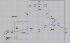
perhaps the input stage can benefit from a resistor that increases the Iq of the very first BJT somewhat.. I made a version like that: see my attachment.. It indeed gives very respectable THD figures... something like -66dB@1KHz@1watt@8ohm
BTW do you use LTspice?
Now let's build that cRaZy thing
Goodluck
PS
Forgot to mention the best improvement I got so far was using the TIP141 instead of 2N3055.
that's a nice update... I get -52dB where you get -57dB Harm2nd...(I use 12dB fundamental for 1Watt in 8Ohm) but my sims THD are usually +/- 10dB compared to real-life.
perhaps the input stage can benefit from a resistor that increases the Iq of the very first BJT somewhat.. I made a version like that: see my attachment.. It indeed gives very respectable THD figures... something like -66dB@1KHz@1watt@8ohm
BTW do you use LTspice?
Now let's build that cRaZy thing
Goodluck
PS
Forgot to mention the best improvement I got so far was using the TIP141 instead of 2N3055.
Attachments
BTW do you use LTspice?
Yes.
Now let's build that cRaZy thing
Having just began work after a long period of unemployment it may be a few weeks before I can order the remaining parts I need but I am anxious to get it going. I have a big hurky power transformer that should do the job and I have some of the small signal transistors, resistors etc and I have a heat sink that should do for a single channel.
Forgot to mention the best improvement I got so far was using the TIP141 instead of 2N3055.
I will check it out and see what I can find out about it. Since I am using more than one I am not locked into the 3055. When I started this all I was planning on using the one 3055 I had but I found that I was going to either have to buy another power transistor or a power resistor (the ones I had were to small) so I figure I might as well just get the trannys that I want to use.
BTW
What do you think of using MJE15031 or 15029 for the PNP output drivers? Do you think that the plastic cased TIP141 will be able to transfer heat to the heatsink well enough to run at a constant 1.5A with a 3"x4" 8 rib heatsink? I was planning on using a TO-3 type device but the plastic case is a little easier to mount.
I don't plan on putting the drivers on the heatsink with the output devices. I thought that I would just make up some bolt on sheet metal "postage stamp" heatsinks for the drivers just to make sure that they remain cool. I think that mounting them on the main heatsink would probably actually heat them up.
Aha job, work, employment!!! good for you . congrats..
Lots of people use the MJE15031 as a driver and according to specs it should do a good job. I am afraid that 30watts of heat dissipation through a small plasitc devices is too much, you really need TO-3 here.
greetz,
Thijs
. congrats.. Lots of people use the MJE15031 as a driver and according to specs it should do a good job. I am afraid that 30watts of heat dissipation through a small plasitc devices is too much, you really need TO-3 here.
greetz,
Thijs
That is what I was thinking. Maybe something like
Regular Transistors ==> MJ15001, MJ15003 or
Darlingtons ==> 2N6284, MJ11016
From the data sheets it looks like the MJ15001 has the most constant hfe at around 1A or less. The Darlingtons seem to vary widely with changes in Ic. I will have to run some numbers and see if I can reduce the bias current a bit to take advantage of the more linear range of the 15001.
As has been metioned se input ss amp topologies have been worked for ~ 40 yrs so it would be surprising to see something completely new
If I have interpreted the “game” rules appropriately the following “simple” se input circuit is in the range of complexity under consideration
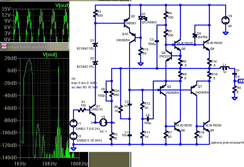
Trying to maximize global negative feedback performance I’ve enhanced the loop gain with cascode Q2,10 and bootstrap current source collector load R11,12, C4
I believe sziklai/cfp pair compound emitter follower Q3,6 was already in play as output stage
Q4,5 (+Q9) form a 750mA(x2 = 1.5A) feedback current source with the “center tapped” current sense R8,9 (+R14,15) giving push-pull class A output to +/- 3 A with all npn output stage; Q4 feedback Q is biased @ 50mA with another bootstrap current source R4,5 C3
Q7,8,9 just parallel the output devices for power sharing, allowing TO-220 plastic output Q without heroic heatsink requirements – it might be desirable to triple the outputs, increasing standing current to 2.2A to drive reactive loads with substantial impedance dips (i.e. real loudspeakers)
C1,2 R14 set dominant the pole while keeping open loop gain flat to 30KHz
R2,20 set a closed loop gain of 20
D1,2 just remove some heat stress from Q1
D4 clamps Q5,9 drive, improving positive clipping behavior (still not great – don’t clip ss amps) ( BAT 54 is too low V rating but is the only small schottky supplied with LTSpice)
DC input bias is included in V1 voltage source, the input impedance @Q1 base is sufficiently high that biasing should be pretty transparent
Loop gain can be explored with AC analysis, plotting V(a)/V(b)
Sim performance is good, -104 dB 2nd, -122 dB 3rd less than 2dB below clipping (which happens at +/- 18 V swing)
LTSpice file, replace .txt with .asc
If I have interpreted the “game” rules appropriately the following “simple” se input circuit is in the range of complexity under consideration
Trying to maximize global negative feedback performance I’ve enhanced the loop gain with cascode Q2,10 and bootstrap current source collector load R11,12, C4
I believe sziklai/cfp pair compound emitter follower Q3,6 was already in play as output stage
Q4,5 (+Q9) form a 750mA(x2 = 1.5A) feedback current source with the “center tapped” current sense R8,9 (+R14,15) giving push-pull class A output to +/- 3 A with all npn output stage; Q4 feedback Q is biased @ 50mA with another bootstrap current source R4,5 C3
Q7,8,9 just parallel the output devices for power sharing, allowing TO-220 plastic output Q without heroic heatsink requirements – it might be desirable to triple the outputs, increasing standing current to 2.2A to drive reactive loads with substantial impedance dips (i.e. real loudspeakers)
C1,2 R14 set dominant the pole while keeping open loop gain flat to 30KHz
R2,20 set a closed loop gain of 20
D1,2 just remove some heat stress from Q1
D4 clamps Q5,9 drive, improving positive clipping behavior (still not great – don’t clip ss amps) ( BAT 54 is too low V rating but is the only small schottky supplied with LTSpice)
DC input bias is included in V1 voltage source, the input impedance @Q1 base is sufficiently high that biasing should be pretty transparent
Loop gain can be explored with AC analysis, plotting V(a)/V(b)
Sim performance is good, -104 dB 2nd, -122 dB 3rd less than 2dB below clipping (which happens at +/- 18 V swing)
LTSpice file, replace .txt with .asc
Attachments
JCX;
That is an interesting design. It is much more complex than what I was looking at but then again this project has gotton more complex each day. I wonder how it would do without the GNF or if it could even be implemented without GNF. It seems that your current sources are dependent on feedback from the output.
The idea of using parallel plastic devices is appealing since it would keep the device current in the range of more constant hfe. I have, however, found that the MJ21196 has a nice flat hfe curve clear up to 3A so I might be able to do well with a single one of those for the output device. I could either use one of those or even a garden variety 2N3055 for the current source.
How would you plan to implement the voltage source at the emitter of Q1? What is the purpose of separating Q1 from its emitter resister through this voltage source? Is this to allow more input voltage swing? Oh wait a minute. You are using DC feedback to the emitter of Q1. So V3 must be to compensate for the DC voltage on the feedback path. Am I close?
I take it that in the actual circuit the bias voltage source would be replaced with some sort of resistive network to bias Q1 yes?
I am trying to understand the reason for the complex current sources that you are using. I admit that I am not familiar with the feedback current source or why one would use it. Can you explain further? If I am following this correctly the output current source is controlled by D4 in conjunction with R4 and R5 to set current. What is the purpose of the bootstrap? Does this configuration act more like a push-pull design than a CCS load? If so that would certainly contribute to lower 2nd harmonic I suppose.
I would expect this type of design to have relatively high 3rd harmonic (compared to the second). To what do you attribute the low 3rd harmonic content?
Thankyou for your patience. As should be obvious I am a greenhorn when it comes to amplifier design but I am anxious to learn.
That is an interesting design. It is much more complex than what I was looking at but then again this project has gotton more complex each day.
I wonder how it would do without the GNF or if it could even be implemented without GNF. It seems that your current sources are dependent on feedback from the output. The idea of using parallel plastic devices is appealing since it would keep the device current in the range of more constant hfe. I have, however, found that the MJ21196 has a nice flat hfe curve clear up to 3A so I might be able to do well with a single one of those for the output device. I could either use one of those or even a garden variety 2N3055 for the current source.
How would you plan to implement the voltage source at the emitter of Q1? What is the purpose of separating Q1 from its emitter resister through this voltage source? Is this to allow more input voltage swing? Oh wait a minute. You are using DC feedback to the emitter of Q1. So V3 must be to compensate for the DC voltage on the feedback path. Am I close?
I take it that in the actual circuit the bias voltage source would be replaced with some sort of resistive network to bias Q1 yes?
I am trying to understand the reason for the complex current sources that you are using. I admit that I am not familiar with the feedback current source or why one would use it. Can you explain further? If I am following this correctly the output current source is controlled by D4 in conjunction with R4 and R5 to set current. What is the purpose of the bootstrap? Does this configuration act more like a push-pull design than a CCS load? If so that would certainly contribute to lower 2nd harmonic I suppose.
I would expect this type of design to have relatively high 3rd harmonic (compared to the second). To what do you attribute the low 3rd harmonic content?
Thankyou for your patience. As should be obvious I am a greenhorn when it comes to amplifier design but I am anxious to learn.
quickly (i'm late, i'm late...)
V3 is just a test V for open loop gain, just a short in a real circuit
V1 has 1.7 V DC offset to bias amp properly - another quick Spice shortcut, yes just use a R divider from pwr supply to Q1_b to set DC, cap couple input signal
in output stage current source circuit Q4 is "error amp" and it's Vbe is the ref that regulates the current in sense resistors R8,9 by controlling Q5 - very common bipolar current source, just in an unusual place, usually Q4 emitter and sense R are at negative rail and regulated output current is taken from Q5 collector, R4,5 supply bias current to Q4, C3 bootstraps the voltage at R4,5 junction to follow the output V, keeping the voltage across R5 constant (and therefore the current through R5 is constant)
while some of the techniques could be used in without global feedback the low harmonic distortion relies on high loop gain reducing the current swing in Q1 to very low levels so that it's exponential Vbe/Ic curve's influence on distortion is reduced - second harmonic from the input Q roughly reduced by the loop gain, input stage 3rd harmonic drops ~ as the square of the loop gain
don’t you hate it when your post is the last on a page
- Status
- This old topic is closed. If you want to reopen this topic, contact a moderator using the "Report Post" button.
- Home
- Amplifiers
- Solid State
- New guy on the block thinking class A