just take a look at this
www.darkfenriz.webpark.pl/mosfet.jpg
what do you think??
to be honest it's my first project of such an amp and I think it;s better than on the 'opamp based mosfet amplifier' forum
any suggestions very welcome
thanks in advance...
www.darkfenriz.webpark.pl/mosfet.jpg
what do you think??
to be honest it's my first project of such an amp and I think it;s better than on the 'opamp based mosfet amplifier' forum
any suggestions very welcome
thanks in advance...
hi darkfenriz
Are you sure that this design is sounding (or even working) fine?
I have some doubts about the auto-bias configuration of the output driver stage (NPN bjt). How does it controls in a stable way the bias current of the mosfets? Driver current is probably a bit low with 22K resistors even if we do not know the VGSoff of the mosfet (type unknown).
What is the purpose of the 22K resistors at collectors of NPN driver bjt (except limit the maximum output swing of the AC voltage thus reducing the maximum possible power of the amp)?
There is no frequency compensation at all in the circuit, I have some doubts on the risk of oscillation...
But, this is only my impressions. Maybe other peoples could comment too.
Fab
Stocker said:the simulator
the simulation
or the circuit
and why not?
Well, if you pencil in the DC voltages without input signal, it'll be clear. Like using your brain as the simulator?
Jan Didden
~some~ of us are at work...
I think it is more constructive to say why/what doesn't work than to just say it doesn't.
Add some toungue in cheek
and you get my commentary / genuine question.
If someone does bother to make the cct work on paper, this is something I just might actually prototype
I think it is more constructive to say why/what doesn't work than to just say it doesn't.
Add some toungue in cheek
and you get my commentary / genuine question.
If someone does bother to make the cct work on paper, this is something I just might actually prototype
Stocker said:[B[snip]I think it is more constructive to say why/what doesn't work than to just say it doesn't.
[snip][/B]
Yes, you are right. But maybe go one step further, and give a hint how to discover yourself why it doesn't work, which I always try to do (not always succeeding). I mean that, I don't want to sound pedantic or anything. That's how I learned it, I had some great prodders when I worked at Philips in my tender years.
They didn't tell me: "your output level is too low". They told me: "what's your output level?". I would measure it, and say "it's too low". They would say, "Really? Why?". I really had to think hard, but I learned lessons I never forgot.
Like that fable, "Give a man a fish, and he has a great meal. Teach a man to catch fish, and he will eat for the rest of his life".
Jan Didden
Stocker said:[BI think it is more constructive to say why/what doesn't work than to just say it doesn't. [/B]
i'm just starting to learn how amps work, so I can't really comment on why that design doesn't work.
It does not work because:
1. The front end of the amplifier is not amplifying anything...but that can be easily corrected. With the values as they are, the front end is a non-inverting unity gain amplifier...the critical mistake is the .1uF cap preventing the voltage divider formed on the - input of the op-amp from seeing 0 potential (ground).
2. The second op-amp is configured as an inverting amplifier (why??) that is incomplete, and must be finished with another resistor to ground to complete the voltage divider that ensures proper gain control of the amplifier...if it is just meant to invert the signal it should just have been left without the resistor between the output and input.
3. The third op-amp is another inverter (why again??), although again improperly configured. The + and - inputs must always have some sort of a path back to each other, you need resistors to bring the inputs to ground if you ground the opposite input.
4. What you are doing with your transitors could be done better a different way. First of all, your bias will be WAY to low to prevent crossover distortion with a 220K to that base, you would be operating in class-B territory as far as I am concerned (bad sound ) It just needs work, bottom line.
5. Thermal feedback is where? ie. The amp heats up and what will compensate for it? I presume you were thinking that the NPN's would do the trick?
This circuit can be done in a simpler fashion and will actually work..
You need to first correct the front-end so that it will actually amplify the signal input to your rails...with a ~ 2V signal input (typical output of consumer players, etc) you need a minimum gain of about 20 in order to obtain a sine of full amplitude when asked to...you could do a gain of 30 which would mean that the output would reach peak when the input is only 1.3333V, which would ensure a loud player, even if average input is lower than 2V.
Skip the inverting unity-gain stages and get right to the transistors.
Make sure you have thermal feedback and compensation because this amplifier will have to be used where that pesky heat is a concern.
Up your bias, so you have more current on the bases of the driver transistors, so you can get a solid class AB out of it.
Add some compensation caps and a damper.
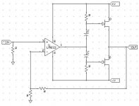
Attached is a VERY simplified version of this....to show the basic working concepts behind the op-amp connection and such. Gain is controlled by that voltage divider accepting the feedback from the output of the amplifier. The grounding resistor of the + input sets input impedance. The caps provide an AC path (audio is AC of course) to the FET's while keeping the DC bias voltage off of the output of the op-amp. The N-channel on top will automatically keep the signal the way it should be, the N-chan is only on with + voltage (ie top of the sine wave) and the P-chan below it is only on when there is - gate voltage (ie bottom of the sine wave). The resistors to the gates provide a DC bias to the FET's to prevent crossover distortion. It needs more stuff to function as a real amplifier in real life, but go ahead and simulate it. For 40V rails, try a 20K bias resistor, use a 10K for the input impedance selection, and a 30K over 1K divider from the output for a gain of 30. It should start to clip at just over 1.3V. Just play around.
I don't understand how you guys can say that it "does not work" if you have no grasp of the concepts behind it....how they should work in the first place. You have scared this guy off with your negative comments, and not one of you could actually help the guy out. I am no EE, but I am posting this because nobody else has posted anything meaningful to this man and I feel that someone should.
-Matt
1. The front end of the amplifier is not amplifying anything...but that can be easily corrected. With the values as they are, the front end is a non-inverting unity gain amplifier...the critical mistake is the .1uF cap preventing the voltage divider formed on the - input of the op-amp from seeing 0 potential (ground).
2. The second op-amp is configured as an inverting amplifier (why??) that is incomplete, and must be finished with another resistor to ground to complete the voltage divider that ensures proper gain control of the amplifier...if it is just meant to invert the signal it should just have been left without the resistor between the output and input.
3. The third op-amp is another inverter (why again??), although again improperly configured. The + and - inputs must always have some sort of a path back to each other, you need resistors to bring the inputs to ground if you ground the opposite input.
4. What you are doing with your transitors could be done better a different way. First of all, your bias will be WAY to low to prevent crossover distortion with a 220K to that base, you would be operating in class-B territory as far as I am concerned (bad sound
) It just needs work, bottom line. 5. Thermal feedback is where? ie. The amp heats up and what will compensate for it? I presume you were thinking that the NPN's would do the trick?
This circuit can be done in a simpler fashion and will actually work..
You need to first correct the front-end so that it will actually amplify the signal input to your rails...with a ~ 2V signal input (typical output of consumer players, etc) you need a minimum gain of about 20 in order to obtain a sine of full amplitude when asked to...you could do a gain of 30 which would mean that the output would reach peak when the input is only 1.3333V, which would ensure a loud player, even if average input is lower than 2V.
Skip the inverting unity-gain stages and get right to the transistors.
Make sure you have thermal feedback and compensation because this amplifier will have to be used where that pesky heat is a concern.
Up your bias, so you have more current on the bases of the driver transistors, so you can get a solid class AB out of it.
Add some compensation caps and a damper.
Attached is a VERY simplified version of this....to show the basic working concepts behind the op-amp connection and such. Gain is controlled by that voltage divider accepting the feedback from the output of the amplifier. The grounding resistor of the + input sets input impedance. The caps provide an AC path (audio is AC of course) to the FET's while keeping the DC bias voltage off of the output of the op-amp. The N-channel on top will automatically keep the signal the way it should be, the N-chan is only on with + voltage (ie top of the sine wave) and the P-chan below it is only on when there is - gate voltage (ie bottom of the sine wave). The resistors to the gates provide a DC bias to the FET's to prevent crossover distortion. It needs more stuff to function as a real amplifier in real life, but go ahead and simulate it. For 40V rails, try a 20K bias resistor, use a 10K for the input impedance selection, and a 30K over 1K divider from the output for a gain of 30. It should start to clip at just over 1.3V. Just play around.
I don't understand how you guys can say that it "does not work" if you have no grasp of the concepts behind it....how they should work in the first place. You have scared this guy off with your negative comments, and not one of you could actually help the guy out. I am no EE, but I am posting this because nobody else has posted anything meaningful to this man and I feel that someone should.
-Matt
Attachments
Hi zagisrule
One the goal of the forum is to gather hints from other peoples to avoid building amps that do not work and may even destroy expensive mosfet output transistors. This is good intention I believe. If you have noticed in my post I have arised some comments and questions about the design which could bring some discussion from any peoples on this forum to maybe eventually make the amp works! So, please do not shoot at peoples comments. Every comments are welcome and may generate new ones too!
Regarding YOUR suggested circuit, you have not indicaed if you had tried it before posting it. Some questions about it:
1- How do you set the bias current (adjust gate voltage) of the output mosfets (by the way the jFET symbol is used instead of mosfet in your circuit)?
2- How do you prevent DC voltage to be present at output of the amp?
3- In general, how does your circuit helps darkfenriz?
Hi darkfenriz
What is your objective in diy?
Since you have used 2 N channel mosfets in your original circuit (quasi-complementay output stage), is it because you already have some parts readily available and you want to use them? In the past, I had obtained about 60 used heavy duty V-mosfet (used in stepping motors) and designed a simple power amp using them. It was not using any op-amp but gave good sounding results with a low overall feedback, THD of < 0.04% and damping factor > 150 (with single pair of mosfet).
Fab
The op-amp would require two resistors to provide DC output protection...acting as a DC servo. The resistors would be placed in parallel to the AC signal capacitors and adjust bias through those resistors.
Bias current would be adjusted with an adittional circuit involving a NPN and PNP transistor, to drive the MOSFET's.
Like I mentioned earlier, that was only a concept schematic, I have not tested it but in theory it would work. I did not have time to draw up a complete schematic, and I thought that my words might have helped him learn more that just giving him a functional schematic. He is trying to do this himself, hence his first attempt, so why not just help him out and let him do some work too? That is the best way to learn.
-Matt
..just thoughts, no simulation, not tested in reality:
1. The overall feedback is not a negative feedback! It is a positive feedback (signal two times inverted) and the gain of the loop is high ==> Amplifier output will probably stick close to positive or negative rail.
2. The bipolar drivers do not give voltage gain, if you pick the signal from the emitter.
3. The biasing of the stages behind the OP amps seems strange to me.
4. No frequency compensation.
5. Overall feedback (after correction of my first point) is setting the AC gain to 2 (6db).
Is this enough?
How to improve?
1. The collectors of the bipolar drivers would deliver the inverted signal, so the overall feedback would become negative, as required.
2. In order to get some gain of the bipolar drivers, we could pick a ratio of about 1/20 between emitter resistor and collector resistor. In first aproach the voltage gain will be Gain=Rcollector/Remitter.
I.e.: 22K at the collector and 1K at the emitter.
3. Difficult, but at least we will need to overcome the 30V...40V difference between the OP amp output and a reasonable operating point of the basis of the lower bipolar. My suggestion: putting a 1uF capacitor in series to the 22k between the lower OP amp and the lower bipolar, in order to get the AC signal, but independend DC operating point. Instead of the 220k between basis of the lower bipolar and ground, we could use a 470k potentiometer between basis and collector. This hould allow to adjust a reasonable idle current.
4. Making one stage dominantly slow (i.e. cap parallel to the feedback resistor of the 2nd OP amp).
Additonal a much smaller capacitor in parallel to the overall feedback resistor from amp output to inverting input may improve, too.
But in fact for such a beast with lot's of OP amps, bipolars and Mosfets inside one strong feedback loop it will be difficult to avoid oscillation.
5. Lowering the value of the 22k which is in series to the groundwards connected 1uF cap allows any desired AC gain.
...hope this brain storming might not cause to much confusion.
Good Luck
Markus
zagisrule, your simplified amp wouldn't work either. The biasing of the output devices cannot be done with those two capacitors. Assuming your JFET symbols are actually meant to be enhancement mode MOSFETs, then for biasing the output devices you should use either a string of forward biased LEDs or diodes, or a couple of reversed biased zeners, or better yet an adjustable Vbe multiplier implemented with another transistor.
Regards,
-Ti
Regards,
-Ti
ChocoHolic said:[B...How to improve?
...
1. The collectors of the bipolar drivers would deliver the inverted signal, so the overall feedback would become negative, as required.
2. In order to get some gain of the bipolar drivers, we could pick a ratio of about 1/20 between emitter resistor and collector resistor. In first aproach the voltage gain will be Gain=Rcollector/Remitter.
I.e.: 22K at the collector and 1K at the emitter.
Markus [/B]
Hi ChocoHolic,
I have an observation/question about your recommendation#1 and #2. Regarding the overall feedback it is a fine observation.
If the gate of the mosfet is connected to the collector of the bjt and the mosfet VGS is something between 0.7 to 4V depending on the mosfet used, then that makes a low dc VCE for the bjt and a lot of voltage across the 22k since the bjt driver stage current would need to provide at least something like 2 ma, thus 22K x 2ma gives 44V (no AC voltage swing across the bjt?)! Maybe I am misunderstanding something here?
Fab
- Status
- This old topic is closed. If you want to reopen this topic, contact a moderator using the "Report Post" button.
- Home
- Amplifiers
- Solid State
- mosfet and opamp amplifier