Hi Damir,
I know you will get totally different results with models of mainstream transistor.
But what are your results if you use my idealized transistor models?
edit: Anyhow, my point was that (theoretically) the distortion of a so called CFA input stage is much lower than from a VFA input stage.
Why? because the CFA IPS doesn't exhibits the tanh x-fer characteristic, it's far more linear.
Cheers,
E.
Last edited:
Hi Damir,
I know you will get totally different results with models of mainstream transistor.
But what are your results if you use my idealized transistor models?
edit: Anyhow, my point was that (theoretically) the distortion of a so called CFA input stage is much lower than from a VFA input stage.
Why? because the CFA IPS doesn't exhibits the tanh x-fer characteristic, it's far more linear.
Cheers,
E.
Hi Edmond, could you put your idealized transistor models as text, I could not copy it from the sim file and if I rewrite it manually I could make mistakes.
BR Damir
No problem:
*** NPN Generic
.MODEL N1 NPN (BF=500 CJC=0p CJE=0p IKF=1 IKR=1 IS=20f ITF=10m MJC=500m
+ MJE=500m RC=1m TR=0n VAF=1k VAR=1k VJC=700m VJE=700m VTF=10 XTF=500m)
*** PNP Generic
.MODEL P1 PNP (BF=500 CJC=0p CJE=0p IKF=1 IKR=1 IS=20f ITF=10m MJC=500m
+ MJE=500m RC=1m TR=0n VAF=1k VAR=1k VJC=700m VJE=700m VTF=10 XTF=500m)
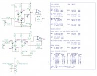
Here I modified my drawing of post #636
I added an ameter, AM15 or AM25, in series with each emitter of the input transistor, T11 for the simplified CFA, T21 for the VFA.
Results are very clear, the input transistors work with equal voltages and currents :
emitter current
CFA --> AM15 873.539 µAdc 88.618 nAac
VFA --> AM25 873.539 µAdc 88.542 µAac
base-emitter voltage
CFA --> VM11 639.91227 mVdc 2.702615 µVac
VFA --> VM21 639.91227 mVdc 2.699602 uVac
base current
CFA --> AM11 8.648904 uAdc 7.534412 nAac
VFA --> AM21 8.648903 uAdc 7.459995 nAac
collector current
CFA --> AM13 864.89033 uAdc 81.083936 nAac
VFA --> AM23 864.89033 uAdc 81.081837 nAac
The output currents of the common node of the feedback resistors R1a-R1b or R2a-R2b are :
CFA --> AM12 97.46077 µAdc 88.618348 nAac
VFA --> AM22 8.479807 uAdc 5.706717 nAac
VFA --> AM25 88.54183 nAac
With the VFA circuit, the buffering action of inverting input transistor T22 provides the same value of AC current to the emitter of input transistor T21 (AM25)as the value of AC current directly provided by feedback network in the CFA circuit (AM12).
In both cases, the input transistors works with the same variations of Vbe and of emitter current.
If the current variation of the input transistor is considered as being the controlling value, then both are CFAs.
If voltage Vbe of the input transistor is considered as being the controlling value of the device, then both circuits are VFAs. I very much prefer this way which is by far easier to use, for example to quickly evaluate thermal influences.
Attachments
Last edited:
Hi Damir,
I know you will get totally different results with models of mainstream transistor.
But what are your results if you use my idealized transistor models?
edit: Anyhow, my point was that (theoretically) the distortion of a so called CFA input stage is much lower than from a VFA input stage.
Why? because the CFA IPS doesn't exhibits the tanh x-fer characteristic, it's far more linear.
Cheers,
E.
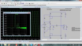
Hi Edmond,
Here with idealized transistors(it sims that idealization work only for FB ).
BR Damir
Attachments
...
it sims that idealization work only for FB ...
BR Damir
Damir
I would think its more apples to apples if you leave the load resistor the same in both cases and adjust in input voltage in the open loop case to result in the same output swing (your simulation has significantly more collector current change in the open loop case).
Thanks
-Antonio
...
Results are very clear, the input transistors work with equal voltages and currents...
Forr,
Try doing the same with a typical cfa complimentary input pair compared to a typical ltp.
For the cfa there is a fixed voltage across the two bases, ignoring the error current flowing into the feedback network (less as this network impedance is increased) then as the input changes the common emitter voltage (the negative input) will also change (a follower) but since there is a constant voltage across the bases the amount of b-e change (in opposite directions) is the same for each transistor. It is the non-linear difference between these b-e voltages than constitutes distortion. Now if you think of these voltages superimposed on the exponential i-v curve of the transistors you will see that given equal and opposite voltage movements from the bias point the resulting change in collector currents for each is significantly different and each is now sitting on a different slope portion of the i-v curve. However it is the difference in these currents which flows through the high impedance gain node and supplies feedback.
In contrast for an ltp, there is no voltage constraint across the bases, but rather a constraint that the sum of collector currents remain constant.
This means that as the input voltage the collector currents will change (equal and opposite amounts). If this is viewed from the same inherent exponential i-v curve then there is an symmetrical delta on the current axis (opposed to the cfa voltage axis) resulting in the inherent non-linear difference in the two be emitter voltages. The difference in these two base emitter voltages is basically the distortion at the feedback point.
The net is an ltp will show much more linear collector currents as a function of vin, with the corresponding exponential appearing as distortion across the base emitters, whereas the cfa will show very linear base emitter changes as a function of vin with the corresponding exponential appearing on the collector currents.
Thanks
-Antonio
Damir
I would think its more apples to apples if you leave the load resistor the same in both cases and adjust in input voltage in the open loop case to result in the same output swing (your simulation has significantly more collector current change in the open loop case).
Thanks
-Antonio
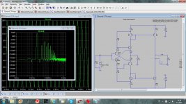
Antonio, you were right. Distortion increases from 0.000016% fot the CFA to 0.000046% for the open loop CC.
Damir
Attachments
One of the reasons for a compl push-pull circuit or other totally symetrical topology is so that the distortion will cancel withOut gnfb. The harmonics shown should be .0000000% open or closed loop If the transistors have exactly the same parameters/characteristics. This is not the case with asymetrical topologies which fundamentally rely on ever more gnfb to reduce (but never can attain zero) distortion.
Do you see my point re topologies? One is inherently more ideal to begin with.
Thx-RNMarsh
Do you see my point re topologies? One is inherently more ideal to begin with.
Thx-RNMarsh
Last edited:
This is only true of even order harmonics and only if your "complementary" devices are ideal. Odd order harmonics are simply reinforced and not cancelled.One of the reasons for a compl push-pull circuit or other totally symetrical topology is so that the distortion will cancel withOut gnfb.
This is only true of even order harmonics and only if your "complementary" devices are ideal. Odd order harmonics are simply reinforced and not cancelled.
the residuals shown dont show that happened. how come? assuming ideal. Open loop -- just a liitle atten of even... not cancelled. why not? same values, same parameters on transistors, symetrical topology. where's the cancellation?
Last edited:
only works for even order distortions - everything has odd too - eventually clipping at symmetircal rails
and its hard to get the evens to match when you are balancing all the differences between N and P type silicon swaping roles in the "complementary" devices
diff pair, Nelson's SUSY work because matching, cancelation with like polarity devices distortion is more robust
and its hard to get the evens to match when you are balancing all the differences between N and P type silicon swaping roles in the "complementary" devices
diff pair, Nelson's SUSY work because matching, cancelation with like polarity devices distortion is more robust
Hi Magnoman,
I should not have put the distorsion results. I have simulated the circuit with a push-pull input stage with good results but it complicated the comparison with a differential input stage.
My aim was not to compare the performances of CFA vs VFA.
I was interested how both circuits work. I think that the shown values of voltages and currents prove that the circuits are fundamentaly governed by exactly the same principle which has already been clearly explained using few but sufficient words in some previous posts.
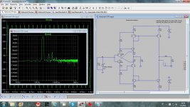
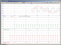
Both camps are wrong. With CFB almost all odd harmonics are cancelled. The 5th harmonic is clearly visible, though THD figures, compared to a VFB stage, are enormously smaller.
THD CFB: 0.7ppm
THD VFB: 1100ppm
edit: the black curve is the residual of the CFB stage. Green is THD of the CFB stage, red is THD of the VFB stage.
Cheers,
E.
THD CFB: 0.7ppm
THD VFB: 1100ppm
edit: the black curve is the residual of the CFB stage. Green is THD of the CFB stage, red is THD of the VFB stage.
Cheers,
E.
Attachments
Last edited:
...
I was interested how both circuits work. I think that the shown values of voltages and currents prove that the circuits are fundamentaly governed by exactly the same principle which has already been clearly explained using few but sufficient words in some previous posts.
Understand I just dont agree. I havent seen anything clearly explaining this.
My previous post (787) although wordy, and likely not entirely clear, contradicts this. Maybe we just aren't talking apples to apples (I'm usually a step behind in these discussions).
Even for the "odd" distortions currently discussed I would expect an ideal cfa to have less resulting distortion that an ltp for the same rationale.
Edmond: Didn't see your post was busy typing. You can go as far as replacing the input transistors with an pure third order term (plus some dc bias) and see the same effect (adding the feedback will return some of the distorted cfa collector currents but you still win when ideal and isolated)
Thanks
-Antonio
Last edited:
CFB galore
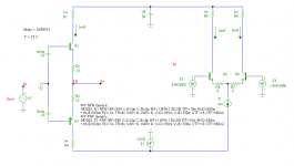
Looking for something else, I stumbled on a five years old design of mine (never built, btw). It not only has a so called CFB input stage, but also a CFB output stage. TMC is also applied two times : at the input- and output stage.
Just another 2 cents.
BTW1, who says that a (so called) CFB amp is inferior?
BTW2, who says you can't apply TMC to a CFB IPS?
And that makes 4 cents.")
Cheers,
E.
Looking for something else, I stumbled on a five years old design of mine (never built, btw). It not only has a so called CFB input stage, but also a CFB output stage. TMC is also applied two times : at the input- and output stage.
Just another 2 cents.
BTW1, who says that a (so called) CFB amp is inferior?
BTW2, who says you can't apply TMC to a CFB IPS?
And that makes 4 cents.
Cheers,
E.
never built, btw
A good reason to claim 0.65ppm THD20 distortions.
- Status
- This old topic is closed. If you want to reopen this topic, contact a moderator using the "Report Post" button.
- Home
- Amplifiers
- Solid State
- Current feedback - Voltage feedback, how do I see the difference?