Both camps are wrong. With CFB almost all odd harmonics are cancelled. The 5th harmonic is clearly visible, though THD figures, compared to a VFB stage, are enormously smaller.
THD CFB: 0.7ppm
THD VFB: 1100ppm
edit: the black curve is the residual of the CFB stage. Green is THD of the CFB stage, red is THD of the VFB stage.
Cheers,
E.


Hi Andrew,
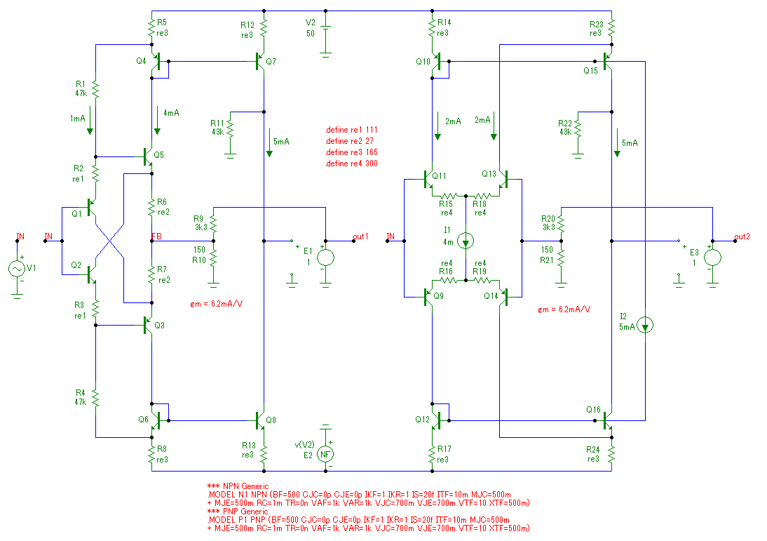
Q3 and Q6 are current sources in order to bias Q4 and Q5. Not only that, they also create a voltage drop across R15 and R16, which supply the base voltage for Q8 resp. Q11.
>cascode
Sure, they are essential for ultra low distortion.
>networks
Just bootstrapping the current sources. This way Vce of Q3 and Q6 is kept constant (to keep Mr. Early outside)
Cheers,
E.
edit: @ Lazy Cat: THX!
Last edited:
A good reason to claim 0.65ppm THD20 distortions.
That's the great thing about sims. You can really do an apple to apple comparison. No b.s.
")
Okay
Cheers,
E.
Edmond , in the VFA schematic , how can a current source
be connected between the two nodal points of the differentials ?...
The upper differential emitters are in principle at 0 - Vbe potential ,
that is about -0.65V , while the bottom side differential emitters
will be accordingly at + 0.65V , that is , the current source is reverse
biaised.....
not exactly offtopic, another current amp: Class-A power amplifier project - Current-Drive - The Natural Way of Loudspeaker Operation
Hi Wahab,
In reality, it can't. Remember, this is just a simulation. Since I'm lazy, why should I draw two current sources, while only one gives exactly the same outcome?
Cheers,
E.
Hi Edmond ,
Well , simulators are wonderfull...
I m quite surprised that ideal devices are used for sims.
Granted that it can be done for CCSs but when it comes to transistors,
that is , the imperfect components that we are stuck with and wich
mandate astucious design , it destroy the whole purpose of simulations.
After all the point is to find the circuit that reduce as much as possible
the components non linearities , so getting rid of them will yield
unrealistical sims that have no practical value.
Back to your schematic , the "CFB" has 150 + 27R degeneration resistor
while the symmetrical differentials are degenerated with about 600R.
In an fair comparison using standard BC546/556 and your schematics
as basis THD results are about the same basicaly , set apart that the "CFB"
has awfull gain/phase response and eventual compensation would certainly
not improve the said THD ratio...
Hi Wahab,
Generally I agree with you.
In this case however, my intention was to show that CFB versus VFB input stages behave radically different and that theoretically a CFB stage gives less distortion. See also post 781 and 796. If you get other results with real components due to imperfections of these components, is certainly not unimportant, but that's another story.
As for a fair and basic comparison, forget the circuit in post 765. Too much components are involved. The simpler circuit in post 796 serves this purpose better, though the distortion of the LTP is flattered because of higher Ic.
If you wish I can repeat the experiment (the simple one) with BC546/556.
Cheers,
E.
The error signal is In, the current entering/exiting the - input.
Further proof that you're wrong can be found on page 13 of the following lecture notes of Dr Tse where he says "to subtract voltage fro voltage, we should use series connection". In other words, since you have a series feedback connection at the input of a so-called "CFA", you are, in fact, subtracting a voltage from a voltage.
http://cktse.eie.polyu.edu.hk/eie304/Feedback.pdf
- Status
- This old topic is closed. If you want to reopen this topic, contact a moderator using the "Report Post" button.
- Home
- Amplifiers
- Solid State
- Current feedback - Voltage feedback, how do I see the difference?