I used two voltage sources in series, one DC and the other pulsating with a sawtooth waveform with rise time of 1ms, a t on of 1ms and fall time of 9ms. This simulates a ripple from a 50Hz mains powered power supply. With a ripple of 7V, I got very high ripple rejection. The distortion figure remained stuck at 0.03% - 0.04%. I also introduced a volume control at the input with a resistance of 10k. For clarity let us assume the variable resistance is made up of two series resistors Rg and Rs where Rg is connected to ground and Rs to the signal source. Rs + Rg = 10k. The output voltage was almost proportional to Rg as expected.
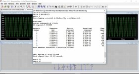
I am simulating an ouput power of 190W into an 8 Ohm load. The distortion at this load is 0.04%. The Frequency response has a cut off frequency at around 100kHz and starts falling at around 13kHz. At 16kHz the drop in dB is around 0.2dB.
At the moment I am trying to add support to more transistor types to LTSpice. I found a list of around 1000 transistor types but adding the list to standard.bjt did not result in the new transistor listed. Any help in this regard is most welcome.
JFTR, I prefer inserting a second voltage source in series just for the ripple instead, avoiding this particular problem. Linear superposition FTW.")
Thanks
That's a method I've never used tbh but it makes a lot of sense.At the moment I am trying to add support to more transistor types to LTSpice. I found a list of around 1000 transistor types but adding the list to standard.bjt did not result in the new transistor listed. Any help in this regard is most welcome.
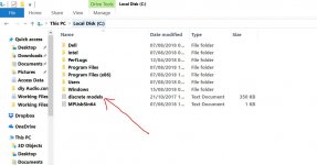
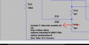
The way I add models is to paste the notepad file containing ALL your additional models directly into the root directory of the C drive having first given it some recognisable easy to use name. I then simply add a .op command to each simulation file saying .include C:\discrete models.txt
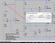
To use any device on the list you simply right click the component (right click the NPN text) and enter a model from your list.
(Maths isn't my strong point I'm afraid... your earlier post)
Attachments
I added the .include directive to the schematic without success. To which file should I add the .include directive? And, from where did you get the transistors list? I have a feeling mine is not in the right format. Is there a way of configuring LTspice to always load added component lists? I tried to add the new transistors to standard.bjt but the new transistors were not recognised and when they were, the parameters were incorrectly read.Mooly said:The way I add models is to paste the notepad file containing ALL your additional models directly into the root directory of the C drive having first given it some recognisable easy to use name. I then simply add a .op command to each simulation file saying .include C:\discrete models.txt
You add it to the schematic itself, as follows:
- click on the .op tool on right hand end of toolbar
- type in: .include modlefilename.typ
don't forget the dot at beginning
- click OK
- the .include command is now floating on your mouse
pointer, place it on the schematic where you want it and click
That's it.
- click on the .op tool on right hand end of toolbar
- type in: .include modlefilename.typ
don't forget the dot at beginning
- click OK
- the .include command is now floating on your mouse
pointer, place it on the schematic where you want it and click
That's it.
I added the .include directive to the schematic without success. To which file should I add the .include directive? And, from where did you get the transistors list? I have a feeling mine is not in the right format. Is there a way of configuring LTspice to always load added component lists? I tried to add the new transistors to standard.bjt but the new transistors were not recognised and when they were, the parameters were incorrectly read.
Its pretty much as EssB says. You add the directive to your simulation workspace as a .op command. Make sure the filepath points to the location of your file.
I've attached the model file I use (which needs pruning because there are duplicates of some devices). At the very top of the page is the filepath I use. That is what I paste (as a .op command) onto each simulation.
You can also paste models into the standard LT library files but that is a method I've never used as it ties the models to that particular installation of LTspice. Its a zipped file because the notepad file is to large to attach directly to the forum.
Attachments
Sadly, I am still unsuccessful notwithstanding I followed all instructions posted in this thread and others that I read online. Somehow, the text file is getting corrupted in a latent way making LTSpice unable to read it without errors. Using the directive ".include drive:\path\to\file" never worked although I tried it many times. I am on version XVII.
While I was trying to add more transistors to LTSpice in Windows, I realised that the LTspice executable file is a 64 bit executable and that it does not use the Windows Registry for its settings. My WINE installation in Linux failed due to unsatisfied dependencies that otherwise break other libraries. So, it was a hopeless case for me to install LTSpice under Linux. But, the 64 bit version of WINE did not have problems installing and running. Realising this, I copied the c:\Program Files\LTC directory to a shared FAT32 partition, rebooted in Linux (Devuan), and copied the LTC directory tree to where wine64 installs its programs. Then, with a bated breath, I tried the bewitched command: "wine64 path/to/LTspice executable" and lo and behold, LTspice appeared on screen.
The way I add models is to paste the notepad file containing ALL your additional models directly into the root directory of the C drive having first given it some recognisable easy to use name. I then simply add a .op command to each simulation file saying .include C:\discrete models.txt
Thanks for this info. I was copying the model text file in the same folder as that of sim file and this was resulting in lot of duplication of files for every sim.
regards
prasi
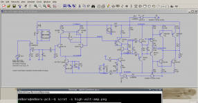
With a common base transistor stage inserted between the differential pair just below the current mirror, results show that a low voltage input stage driving a high voltage output stage can be implemented. The output offset voltage is however too high at around 90mV. I also found that the amplifier is very sensitive to the VAS's primary stage bias resistors. I am attaching a screenshot of the circuit as shown in LTSpice under Linux.
How can the offset voltage be tamed down to a few millivolts?
Thanks.
How can the offset voltage be tamed down to a few millivolts?
Thanks.
Attachments
I would like to beg rispondents to this thread pardon for always posting images instead of the real .asc LTSpice files. Yes, it is a stupid omission, as posting the real file, instead of a picture, not only uses less server resources, but is more useful for anyone wanting to respond.
I used the option:
.option numdgt=7
.option setwinsize=0
but I did not get those mouth-watering low distortion figures. What I am getting is around 0.02% which is good even for commercial amplifiers. This amplifier uses a common base stage to interface a low voltage input stage with a high voltage VAS. Surprisingly, the solution was to use a simple common base stage embedded between the two heads of the differential pair input stage. Since, the current mirror enforces equality of currents reaching the low +V rail, any difference in currents, must be directed through the common base stage.
I found that instability problems, were greatly reduced with this setup. Yes, as expected, there are more instability issues compared with an amplifier using the same rail voltages throughout all three stages, but these problems are far less pronounced compare to using additional interfacing amplifier stages.
I tried the 20kHz square wave test but didn't get it right. It seems the slew rate is low, but the AC analysis shows that the amplifier cuts off at around 100kHz. I extended the analysis up to around 1 or 2 Giga Hertz, but something tells me this is like cases of extreme extrapolation.
Attachments
I had a quick look yesterday at the diagram you posted. Was going to say that one way of always getting zero offset is simply to use a servo... I see you've altered/added resistors in the latest version.
If you are just chasing numbers then the so called 'Blameless' popularised by Doug Self is hard to beat.
If you are just chasing numbers then the so called 'Blameless' popularised by Doug Self is hard to beat.
Attachments
I am not chasing numbers, but I am after getting the simplest amplifier circuit, which can drive a large (~500W continuous) power stage comprised of 4 pairs of 2SC5200 and 2SA1943 power transistors. Using a linearising transistor to linearise the VAS amplifier transistor, the resultant circuit was so stable that it did not require a Miller compensating capacitor. I simulated signals at 1000Hz, 2000Hz, 8000Hz, 16000Hz and 20000Hz. The distortion figure was around 0.2%. I am attaching the .asc file for anyone wanting to give a helping hand by indicating possible problems in the circuit.I see you've altered/added resistors in the latest version.
If you are just chasing numbers then the so called 'Blameless' popularised by Doug Self is hard to beat.
I plan to keep the protective circuitry outside the feedback loop. To dectect current overload, I will use a very low resistance connected to output ground with the other terminal connecting to speaker ground. To detect clipping or better that clipping danger is imminent, I will use two resistors in series connected in parallel with the output load. A separate circuit will process signals from three nodes: power supply, output, and voltage across the very low resistance.
Attachments
I did some minor tweaks to the posted circuit just above. Two biasing 100 kOhm resistors were used to pull up the driver stage's bias in an effort to reduce cross-over distortion. The ouput waveforms show that cross over distortion has been greatly reduced. The other tweak consists of a reduced resistance value across the VAS's driver transistor base-emitter junction. There were very high frequency harmonics superposed on the output signal. This resistor's new value blocked them.
I would like someone to conduct a square wave test to this amplifier circuit. Till now, I have failed to get a such a test that looks good: the fall time is too long, and before the circuit passes all tests, I am hesitant to build it.
I would like someone to conduct a square wave test to this amplifier circuit. Till now, I have failed to get a such a test that looks good: the fall time is too long, and before the circuit passes all tests, I am hesitant to build it.
Attachments
Last edited:
Nevermind, it seems, the circuit shown just above also passes the square wave test at 20kHz.
Thanks to everyone and particularly this forum for empowering me with knowledge to design this amplifier.
Power at 8 Ohm load resistance: 250W (continous)
Distortion at this power: 0.09%
Crossover distortion: virtually eliminated. Output waveform for a sine wave tends to a straight line near crossover (i.e. 0V)
An amplifier that burns expensive speakers in the event of a blown fuse is something to be avoided. Simulating a blown fuse on the positive and negative supply rails resulted in the output clamping at the negative rail voltage. A blown fuse at the negative rail did not result in a clamp with only a few milliamps passing through the speaker. So, I must find a way of avoiding this clamp happening.
I will turn my attention to designing the power supply part where the rectifier bridges are installed. The toroidal transformer has two centre tapped secondaries with voltages of 120V across both coils. Since the original design had the smoothing capacitors on the amplifier PCB, and I will keep the power supply part and amplifier power stage, I think, it is better to place the fuses on the rectifying PCB. This means, current will first flow through a fuse and then it will charge the smoothing capacitors. With this arrangement fuses will be subjected to current spikes from the rectifier bridges, and, I think, the fuses' rating will be higher than the case a smoothed DC current were to flow through them.
What do you think? I aim at having BOTH power supply rails protected by fuses.
Well I used to own a Pioneer A80 (150 wrms) that ran on rails of -/+57 and -/+80 volts (it had a class G output) and I was amazed that none of the high current rails to the output stages were fused.
The protection in the event of output stage failure came from the use of correctly specified fusible emitter resistors and also fusibles fitted to protect the front end rails (in case of a cap going short I suppose). So although it had no fuses, it was fully protected.
I also assume that the event of the bridge failing short circuit would then result in blowing of the 6.3A primary fuse.
I have modified the posted schematic to enable the amplifier thus depicted to use voltages from +/-30V to +/-80V. My aim is to use a low voltage supply when I need low power outputs and to use the full voltage when I need more power. In a home environment a few watts seems enough for me, and for that, an operating voltage of 80V is a waste of energy and an unnecessary stress on components.
Attachments
- Home
- Amplifiers
- Solid State
- My attempts at a design of a 3 stage amplifier