Re: Hello Hugh, where's my bootstrap
I must be missing something in the comments below. What does this have to do with the current discussion???
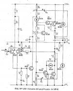
Carver did an interesting thing on the ouput on some of his amps where he feeded some of the output signal into the Bias Transistor CCT.... check out C7 on the following http://ns.netlynx.us/audio/phaselinear/pl400/PL400.gif
-----------------------------------------------------------------------------------
I must be missing something in the comments below. What does this have to do with the current discussion???
Carver did an interesting thing on the ouput on some of his amps where he feeded some of the output signal into the Bias Transistor CCT.... check out C7 on the following http://ns.netlynx.us/audio/phaselinear/pl400/PL400.gif
-----------------------------------------------------------------------------------
destroyer X said:I am crazy to have my bootstrap to feel that outstanding sound some people told me.
Im my idea, can kick me with the boot, or with the strap, and i still crazy to put my hands over this wonder.
My friends is trying to corrupt me, they want to see schematics, they want to put on Ray X....and i said no!...Hugh do not want that!
- But Hugh will never know!
- But my conscience will know!
They are entirely crazy to our meeting to judgement.... we always make this as our fun.... we order to 30 years prison to some Harman Kardon.... we send to electrical chair some Pionner... we are really bad!...leach is already buried... today not more than sand!(the amplifier, long life to Mr. Leach!)
They saw your picture , and they say to me that you are in the middle of the ocean , pointing the skies, with .30 to destroy the airplane that is sending your AKSA 55 kits to damn Destroyer.
They said you are alike one old movie, one strabic (eyes convergence) German soldier trying to shot many airplanes he could see because the strabic eyes.... he said you do not put nothing in mail to me, that i loose money.. inside the pack is one stone!.... they are nervous with me , because i told them cannot see board circuit...only take a look with big distance and without turn it... and they told you made sandwiched boards with capacitors and resistor in the middle.
We are turning crazy (already i am) to see AKSA modules and to hear aksa sound.
Please, do not explode the airplane is bringing modules to me..I will not let them convince me.
No problems with customs, my wife is a graduate customs officer, and i have a lot of Federal Policeman Friends...no way to arrest my circuits, i think it is more easy that they bring here into my hands.
Have you heard about Lula?.... second degree cousin. hohohô
Carlos
markp said:
Yes, but it looks sooo good!
But seriously, I only design complimentary symmetrical drive circuits for my amps. They work well for me. I often drive them with a higher voltage than the output stage to get what I want out of them.
I suspect subjectivists would take issue with this viewpoint on the grounds that 'sonics' are of infinitely more value than 'looks'.......
Re: Re: Hello Hugh, where's my bootstrap
That is frequency compensation, and it is very common.
lubbie said:Carver did an interesting thing on the ouput on some of his amps where he feeded some of the output signal into the Bias Transistor CCT.... check out C7 on the following http://ns.netlynx.us/audio/phaselinear/pl400/PL400.gif
That is frequency compensation, and it is very common.
Yes, C7 is just a phase lead capacitor for frequency compensation. Actually, in that PL400 circuit I'm more surprised by the fact that the bottom of bootstrap cap C11 is not connected to the output of the amp but to the emitter of the top driver. I wonder whether it behaves any different.
Steven
Steven
Steven..
Initially i thought the position of the bootstrap was normal until you metioned it.. I looked around and where carver had put it is very uncommon compared to the amps i've researched. I wonder how the amp would respond if i changed it....
Maybe i see a mod on two Phase Linear 400's in my future.. LOL.. Just so everyone knows, the phase linear on the link is a very early model of 400.
The day i turn myself lucky enougth to find highly matched NPN and PNP units to
a double differential i will do a test usind double VAS, double differential and double bootstrapp.
Also will use double output.... parallel output...more pairs...one pair inside the NFB line and the one connected to the speaker out from the NFB.
It may sound interesting.... i like this Argentine design you offer to us Geirin.
regards,
Carlos
"Actually, in that PL400 circuit I'm more surprised by the fact that the bottom of bootstrap cap C11 is not connected to the output of the amp but to the emitter of the top driver. I wonder whether it behaves any different."
There is no bias current flowing in the output stage, so the bootstrap cap is hooked to the driver stage.
There is no bias current flowing in the output stage, so the bootstrap cap is hooked to the driver stage.

djk said:"Actually, in that PL400 circuit I'm more surprised by the fact that the bottom of bootstrap cap C11 is not connected to the output of the amp but to the emitter of the top driver. I wonder whether it behaves any different."
There is no bias current flowing in the output stage, so the bootstrap cap is hooked to the driver stage.
Hi djk,
You may be right that there is no bias current in the output stage. Dissipation in the drivers Q11 and Q12 would be quite high (5W) before significant bias current in Q13-18 starts to flow. On the other hand, the bias loop contains R41 (0.22). This makes sense if at least some bias current is flowing in the output stage.
But even if there would not be any bias current in the output stage, the minus side of C11 could have been connected at the output of the amplifier, the output impedance is still very low and able to drive the bootstrap capacitor. Also the drivers contribute to the output.
I think the main reason for connecting C11 to the emitter of the driver is that this emitter voltage follows the AC signal on the collector of Q5 much better than the output does, so the voltage across R18 is kept more constant and the collector impedance of Q5 becomes higher and more linear. I think even harmonic distortion is lower because the half wave rectified (class B) non linearity of the voltage across emitter resistors R40, 43, 45 is not fed back.
Steven
I found that the original circuit link was not accessible anymore, so I attach it again.
Attachments
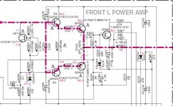
GEirin said:Bootstrapp R250+R249 // R266+ D207.
What is the function?
During clipping of the negative half wave the driver transistor Q220A is cut off. When this happens the voltage potential at its base “rises higher” than what the rail voltage is. (In case of negative rail the “higher” means that the base voltage gets more negative than the rail voltage). Consequently, the diode (along with its series resistor) will limit the base voltage to a value that is only slightly higher than the collector (rail) voltage. This reduces the storage effect and allows the driver transistor to be cut off faster. This in turn reduces cross conduction and therefore protects the transistors.
- Home
- Amplifiers
- Solid State
- Why bootstrap?