PARTLY SOLVED! Oscillation problem with my power amp
EDIT (03.09.2018.):
The oscillation on negative clipping is only about 1V p-p now, when the amp output is unloaded. Very significant improvement, as we started at a frightening 30V p-p! The problem gets somewhat worse with certain loads, but it is already acceptabe to me. Simply said, it is not adviceable to overdrive this amp into clipping. With the intended +/-53V supply voltage, it's absolutely unlikely that anyone will drive it to clipping even in a very big living room.
Otherwise the amp has low harmonic and intermodulation distortion (see #129).
What I heard as annoying in it's sound is perhaps only me myself being too critical and it belongs to the field of psychology. For example, I thought that I clearly heard a significant difference between the Miller and TPC compensations in favor of the Miller. But since I have made the two compenstion methods easily switchable in the amp, and I can change between the two anytime during listening to music, I had to realize that I can't hear any difference at all when swithing from one to the other during passages that seemed to me different before.
Thank you all who took part in helping me!!!
EDIT (05.07.2018.): I wanna thank you all who tried to help solve the problem with my amp.
The "rail override" was due to uncalibrated 10:1 oscilloscope probe.
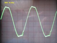
The oscillation which was about 30V p-p or even worse and occured only at negative clipping, has been largely eliminated, it's about 3V p-p now, no risk to damage any speaker. Details at post #28. However this 3V p-p oscillation at around 1MHz freq. can still radiate RF noise via the speaker cable. The two measures that worked (see post #28), cannot be taken any further. The only remedy left seems increasing Cdom but I'd like to avoid that if possible, because the high loop gain (currently ULGF is about 0.9MHz) is the only thing that can keep output stage crossover distortion low. So if you can still advice something else to eliminate the remaining oscillation, please read on! (output transistors are MJL4281 and MJL4302 -- not MJL3281 and MJL1302 as shown on my schematic!!!)
Hi, I hope some of you have run into similar problems and will help me.
I decided to make an amplifier similar to Self's Blameless amp with some differences many of which was advised in Bob Cordell's Designing Audio Power Amplifiers book. I chose to use a EF2 output stage because I'm not so familiar with board layout, and it was said to have less oscillation problems than EF3 and CFP.
The differences to the Blameless:
- 2 pairs of OPTs
- separate heatsink for driver transistors with it's own temp. sens diode
- base stopper resistors on drivers and OPTs
- capacitor multipliers added to supply the IPS-VAS
- TMC compensation (although temporarily made into Miller comp. for the testing)
- a high frequency RC filter (0.68R-220pF) on the supply lines between OPTs and drivers
- separated current source for IPS and VAS
- VAS emitter resistor decreased to 2.2R
- Baker clamp diode on VAS
- rail catching diodes
The OPTs are MJL4281 and MJL4302. LTSpice simulations of the circuit showed that stability problems start only below 15pF Miller cap value (2.5MHz ULGF). So I decided to try 39pF (0.9 MHz ULGF) to allow for wire inductances, tolerances and other non-ideal things.
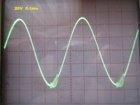
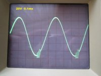
I assembled the PCB I designed, and unfortunately it oscillates very heavily on negative clipping (it's the same both unloaded and with 68R load). If I remove one of the output transistor pairs, or if I increase the Miller cap to 75pF, then the oscillation is less severe, but still there, and then we're already down to 0.5 MHz ULGF and I hoped about 1 MHz for these fast output transistors. I'd like higher ULGF to more efficiently suppress the OPS crossover distortion.
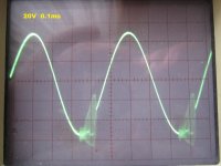
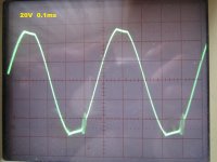
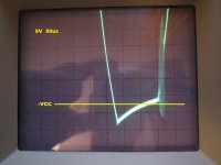
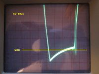
THIS "PROBLEM" HAS BEEN SOLVED: Another extremely strange thing is that on clipping higher frequency (above let's say 400Hz) signals, the clipped output voltage starts to raise above +VCC and to fall below -VCC. By as much as several volts (!) if the slew rate of the clipped signal is high enough! See attached images of 2kHz clipped signal (VCC was +/-50V). This "rail override" of the output voltage just shouldn't be possible due to the rail catching diodes even if there was inductive flyback! But it's the same without load or with 68R resistive load. (I have only a 68R 20W test resistor available right now that can withstand the max. output swing.) So I have no idea what's going on here!!! Simulation shows about +/-45V clipped output with +/-50V VCC. On my prototype I can easily measure +/-55V clipped output or even more while the VCC remains +/-50V. There is some HF noise on the +/-VCC lines while clipping but where does this 10 Volts or more extra output drive come from?
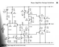
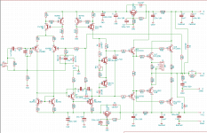
Notes for the LDAmp schematic. On my prototype board: The TMC resistor (R17) was removed. D4 and D5 are short circuited and a 2.4k resistor is fitted between the base of Q11 and the base-collector of Q12. Output transistors are MJL4281 and MJL4302 -- not MJL3281 and MJL1302.
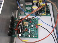
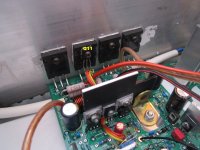
By looking at the schematic Istvan Gerencser has shared 1 photo with you! | Flickr, and layout Istvan Gerencser has shared 1 photo with you! | Flickr, oscilloscope images, any suggestions what causes this "rail override" and what can be done to stop the oscillation without further increasing the Miller cap? The driver transistors are quite far from the outputs because of the separate heatsink...
Oscillation frequencies was measured as follows (approx.):
1output pair with 75pF Miller cap: 1.65 Mhz
2output pairs with 75pF Miller cap: 1.4 MHz
1output pair with 39pF Miller cap: 1.25 Mhz
2output pairs with 39pF Miller cap: 0.85Mhz
regards
gerenis
EDIT (03.09.2018.):
The oscillation on negative clipping is only about 1V p-p now, when the amp output is unloaded. Very significant improvement, as we started at a frightening 30V p-p! The problem gets somewhat worse with certain loads, but it is already acceptabe to me. Simply said, it is not adviceable to overdrive this amp into clipping. With the intended +/-53V supply voltage, it's absolutely unlikely that anyone will drive it to clipping even in a very big living room.
Otherwise the amp has low harmonic and intermodulation distortion (see #129).
What I heard as annoying in it's sound is perhaps only me myself being too critical and it belongs to the field of psychology. For example, I thought that I clearly heard a significant difference between the Miller and TPC compensations in favor of the Miller. But since I have made the two compenstion methods easily switchable in the amp, and I can change between the two anytime during listening to music, I had to realize that I can't hear any difference at all when swithing from one to the other during passages that seemed to me different before.
Thank you all who took part in helping me!!!
EDIT (05.07.2018.): I wanna thank you all who tried to help solve the problem with my amp.
The "rail override" was due to uncalibrated 10:1 oscilloscope probe.
The oscillation which was about 30V p-p or even worse and occured only at negative clipping, has been largely eliminated, it's about 3V p-p now, no risk to damage any speaker. Details at post #28. However this 3V p-p oscillation at around 1MHz freq. can still radiate RF noise via the speaker cable. The two measures that worked (see post #28), cannot be taken any further. The only remedy left seems increasing Cdom but I'd like to avoid that if possible, because the high loop gain (currently ULGF is about 0.9MHz) is the only thing that can keep output stage crossover distortion low. So if you can still advice something else to eliminate the remaining oscillation, please read on! (output transistors are MJL4281 and MJL4302 -- not MJL3281 and MJL1302 as shown on my schematic!!!)
Hi, I hope some of you have run into similar problems and will help me.
I decided to make an amplifier similar to Self's Blameless amp with some differences many of which was advised in Bob Cordell's Designing Audio Power Amplifiers book. I chose to use a EF2 output stage because I'm not so familiar with board layout, and it was said to have less oscillation problems than EF3 and CFP.
The differences to the Blameless:
- 2 pairs of OPTs
- separate heatsink for driver transistors with it's own temp. sens diode
- base stopper resistors on drivers and OPTs
- capacitor multipliers added to supply the IPS-VAS
- TMC compensation (although temporarily made into Miller comp. for the testing)
- a high frequency RC filter (0.68R-220pF) on the supply lines between OPTs and drivers
- separated current source for IPS and VAS
- VAS emitter resistor decreased to 2.2R
- Baker clamp diode on VAS
- rail catching diodes
The OPTs are MJL4281 and MJL4302. LTSpice simulations of the circuit showed that stability problems start only below 15pF Miller cap value (2.5MHz ULGF). So I decided to try 39pF (0.9 MHz ULGF) to allow for wire inductances, tolerances and other non-ideal things.
I assembled the PCB I designed, and unfortunately it oscillates very heavily on negative clipping (it's the same both unloaded and with 68R load). If I remove one of the output transistor pairs, or if I increase the Miller cap to 75pF, then the oscillation is less severe, but still there, and then we're already down to 0.5 MHz ULGF and I hoped about 1 MHz for these fast output transistors. I'd like higher ULGF to more efficiently suppress the OPS crossover distortion.
THIS "PROBLEM" HAS BEEN SOLVED: Another extremely strange thing is that on clipping higher frequency (above let's say 400Hz) signals, the clipped output voltage starts to raise above +VCC and to fall below -VCC. By as much as several volts (!) if the slew rate of the clipped signal is high enough! See attached images of 2kHz clipped signal (VCC was +/-50V). This "rail override" of the output voltage just shouldn't be possible due to the rail catching diodes even if there was inductive flyback! But it's the same without load or with 68R resistive load. (I have only a 68R 20W test resistor available right now that can withstand the max. output swing.) So I have no idea what's going on here!!! Simulation shows about +/-45V clipped output with +/-50V VCC. On my prototype I can easily measure +/-55V clipped output or even more while the VCC remains +/-50V. There is some HF noise on the +/-VCC lines while clipping but where does this 10 Volts or more extra output drive come from?
Notes for the LDAmp schematic. On my prototype board: The TMC resistor (R17) was removed. D4 and D5 are short circuited and a 2.4k resistor is fitted between the base of Q11 and the base-collector of Q12. Output transistors are MJL4281 and MJL4302 -- not MJL3281 and MJL1302.
By looking at the schematic Istvan Gerencser has shared 1 photo with you! | Flickr, and layout Istvan Gerencser has shared 1 photo with you! | Flickr, oscilloscope images, any suggestions what causes this "rail override" and what can be done to stop the oscillation without further increasing the Miller cap? The driver transistors are quite far from the outputs because of the separate heatsink...
Oscillation frequencies was measured as follows (approx.):
1output pair with 75pF Miller cap: 1.65 Mhz
2output pairs with 75pF Miller cap: 1.4 MHz
1output pair with 39pF Miller cap: 1.25 Mhz
2output pairs with 39pF Miller cap: 0.85Mhz
regards
gerenis
Attachments
-
 39p 2OPpairs.JPG152.5 KB · Views: 764
 -
 LDAmp+PS.JPG318.5 KB · Views: 271
 -
 LDAmp_on_heatsink.JPG284.2 KB · Views: 277
 -
 75p 2OPpairs clip.JPG140.2 KB · Views: 156
 -
 75p 2OPpairs.JPG163.6 KB · Views: 815
 -
 39p 1OPpair clip.JPG169.5 KB · Views: 669
 -
 39p 1OPpair.JPG144.2 KB · Views: 703
 -
 39p 2OPpairs clip.JPG160.9 KB · Views: 705
Last edited:
In my experience, clipping misbehavior on one rail but not the other, is often due to extreme output voltage from the current mirror load in the first stage. When the current mirror's output voltage is gigantic, the VAS transistor can go into saturation. When its |Vbe| >> |Vce| , severely ugly things often happen.
The good news is, the circuit almost always misbehaves in simulation, too. So you can overdrive the simulation into clipping, and watch as everything goes straight to hell. You can probe the voltage waveforms and current waveforms to your heart's content.
The usual fix is to limit ("clamp") the output voltage swing of the input stage. Bob Cordell's power amp book shows this on page 63 and numerous later figures. The clamp is transistor Q13. I'm sure Douglas Self's APAD book discusses the same circuit as well, perhaps giving Q13 a different part designation.
Attachments
I usually find that oscillation at clipping needs to be prevented by clamping the VAS and/or current source, not the input stages. Many textbooks show how a couple of diodes can provide anti-saturation. That is usually because saturation generates a phase inversion when the transistor is no longer inverting, so the feedback becomes positive.
Hi Mark! Thanks for the suggestion. But I think it's not the problem, the Baker clamp diode (D3 on my schematic) is there to prevent saturation of the VAS. It diverts current from the base to the collector of the VAS if it would try to saturate. I also removed and installed this diode but no change.
I think the clamp transistor primarily there to prevent overcurrent of the VAS when there is clipping with a very low load (e.g. output short circuit) or when a VI limiter works. In these cases the VAS transistor draws high current and can be damaged. In my circuit there is no VI limiter. And if there is an output short circuit, the OPTs and drivers are more likely to blow first and not the VAS. So I didn't install the clamp transistor. Well I might try the clamp transistor, but I'm almost sure it does nothing about the oscillation...
I think there is some very fundamental, very gross problem that I can't see. The output voltage rises well above +VCC and well below -VCC when the input is overdriven with signals with high enough slew rate, and this thing just seems to be totally impossible. The same if loaded by 68R or unloaded. So something very weird is happening here, the Emitter of NPN output and driver transistors goes several volts above their collectors (+VCC), and the the Emitter of the PNP output and driver transistors goes several volts below their collectors (-VCC) when the slew rate of the clipped signal is high enough. When the slew rate is lower, for example a 100Hz sine wave clipping then there is no "rail override", output remains between +VCC and -VCC.
I began thinking that my old analog oscilloscope might be faulty, because such a high output swing is just impossible. How does the output go HIGHER by 5...10V than +VCC at clipping? Simulation showed that it should stay BELOW +VCC by about 5V. (The same phenomenon, only inverted, on negative clipping.)
It is also strange that the positive clipped output voltage starts higher and then falls toward the +VCC in a manner like a capacitor discharging through a resistor... (The same phenomenon, only inverted, on negative clipping.) See the oscilloscope images I posted yesterday.
I also double checked the transistor pin assignments on the PCB (thought that some Emitter and Collector might have been swapped unintentionally)... But they were fine.
Otherwise the amp seems to work fine until clipping, and I listened to music with it. The highs are a bit too metallic for my taste and the transients like beats and drums sound a bit strange and exaggerated to my taste. Otherwise it sounds OK, and I can hear more details with this amp than with other amps that I listened to before.
I plan to take it to one of my acquaintances who has a distortion meter, but first I want to solve the oscillation problem.
It's also true that there is some weak HF oscillation or spikes on the +VCC and -VCC rails during clipping, about 5V p-p, but it's very smeared and hard to see on my analog oscilloscope.
Hi John Ellis! So the Baker clamp diode I use on the VAS (see my shematic
Can you name a textbook that deals with this?
An externally hosted image should be here but it was not working when we last tested it.
) is not enough? There is no change whether I remove or install this diode...Can you name a textbook that deals with this?
No it's not working. Let's try as link:
sch Istvan Gerencser has shared 1 photo with you! | Flickr
board Istvan Gerencser has shared 1 photo with you! | Flickr
sch Istvan Gerencser has shared 1 photo with you! | Flickr
board Istvan Gerencser has shared 1 photo with you! | Flickr
There is nothing special at R26 and R27, the waveform is much the same as the output except that it goes higher by about 1.5V on positive swing (R26) and lower by about 1.5V on negative swing (R27) than the output.
Unfortunately I cannot measure signals refrenced to other points than ground because I have no differencial probe. So this 1.5V is only very approximate, but it's about two Vbe drops as can be expected.
What totally puzzles me is how the VAS is able to drive the OPS so much higher and lower than the power rails even through the capacitance multipliers that drop about 1V relative to the +/-VCC... And how the output can "disregard" the rail catching diodes...
Maybe I will remove the capacitance multiplier to see if there's any change... Although it seems to be working fine...
I suspect your 2.2 ohm emitter resistor in the VAS is too low. One purpose is to reduce the gain but it increases the frequency response. Conversely, too low and the frequency response is lower. Self suggested a 10 ohm resistor MAY help. I've found 10 ohms to be the minimum and even higher might be needed. Suggest you try 10 ohms but then you could also replace the 680 by 1k to partially offset the gain reduction.
If that does not work you can always add a sprog stopper - typically 100pf- across the BC junction of the PNP driver transistor (as that is where the oscillation is occurring).
If that does not work you can always add a sprog stopper - typically 100pf- across the BC junction of the PNP driver transistor (as that is where the oscillation is occurring).
A while back I had a similar problem and you may find this thread useful-
I need a cure- oscillations at clipping
Alas, I didn't get back to it for a while and apologize to everybody who gave some good answers. They did not, however, go unnoticed or unread. Ultimately I improved things "enough", but not to where I was truly happy with the clipping performance.
I need a cure- oscillations at clipping
Alas, I didn't get back to it for a while and apologize to everybody who gave some good answers. They did not, however, go unnoticed or unread. Ultimately I improved things "enough", but not to where I was truly happy with the clipping performance.
Thanks all who care about my case!
Hi John Ellis!
Yes, I'm gonna try a bigger emitter resistor on the VAS, like 22 Ohms. I chose 2.2R because I didn't want to protect the VAS transistor, and LTSpice showed increased distortion with higher resistances. But the VAS is a transconductance stage so the emitter resistor (I think) behaves differently than in a voltage amplifier stage.
Thanks Conrad, I have already read through that thread.
Hi chip_mk!
Yes, I have tried other GND points although usually connected the GND clip to the heatsink of the bridge rectifier that connects to the star ground through the ground plane of the power supply. But if I connect to the star point or to the decouple ground or to the IPS-VAS's "quiet" ground doesn't seem to make any change in the look of the output waveform.
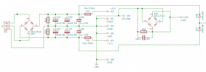
The power supply is very simple, attached image is the part of the PS schematic that is in work. (There was a solid state relay in there I deleted because that is bypassed for now.)
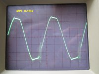
Other attached images is some close up on the output waveform as the amp is clipping a 2kHz sine wave, the output voltage goes well below the -VCC by as much as 7 Volts. Load is 68R. (The positive clipping is very similar without the HF oscillation.) Still have not the faintest idea where this excess voltage comes from that enables the VAS to drive the output below -VCC and how the output gets to go below -VCC. There is no excess voltage on the VCC supply lines except some slight HF oscillation between 2V p-p and 4V p-p (dependient on how hard the clipping is) and approx. symmetrically on the average VCC voltage. The OPS decouple ground also has a slight HF oscillatory component like 2...4V p-p and approx. symmetrical about the average decouple GND voltage. These are hardly visible though on my oscilloscope. I was thinking if the VCC and decouple GND HF oscillations are out of phase, they can add up and provide some 4...8V p-p HF wave superimposed on the VCC rails (relative to OPS decouple GND). But this still doesn't explain what makes the output swing well outside the rails possible? And how does it get through the capacitance multiplier to the VAS? Maybe this my idea is totally wrong, and THERE IS BLACK MAGIC INVOLVED HERE
Anyone any idea how the output can swing OUTSIDE the VCC rails by 7 Volts. Simulation shows the clipped output voltage should be INSIDE the VCC rails by about 5 Volts...
Hi John Ellis!
Yes, I'm gonna try a bigger emitter resistor on the VAS, like 22 Ohms. I chose 2.2R because I didn't want to protect the VAS transistor, and LTSpice showed increased distortion with higher resistances. But the VAS is a transconductance stage so the emitter resistor (I think) behaves differently than in a voltage amplifier stage.
Thanks Conrad, I have already read through that thread.
Hi chip_mk!
Yes, I have tried other GND points although usually connected the GND clip to the heatsink of the bridge rectifier that connects to the star ground through the ground plane of the power supply. But if I connect to the star point or to the decouple ground or to the IPS-VAS's "quiet" ground doesn't seem to make any change in the look of the output waveform.
The power supply is very simple, attached image is the part of the PS schematic that is in work. (There was a solid state relay in there I deleted because that is bypassed for now.)
Other attached images is some close up on the output waveform as the amp is clipping a 2kHz sine wave, the output voltage goes well below the -VCC by as much as 7 Volts. Load is 68R. (The positive clipping is very similar without the HF oscillation.) Still have not the faintest idea where this excess voltage comes from that enables the VAS to drive the output below -VCC and how the output gets to go below -VCC. There is no excess voltage on the VCC supply lines except some slight HF oscillation between 2V p-p and 4V p-p (dependient on how hard the clipping is) and approx. symmetrically on the average VCC voltage. The OPS decouple ground also has a slight HF oscillatory component like 2...4V p-p and approx. symmetrical about the average decouple GND voltage. These are hardly visible though on my oscilloscope. I was thinking if the VCC and decouple GND HF oscillations are out of phase, they can add up and provide some 4...8V p-p HF wave superimposed on the VCC rails (relative to OPS decouple GND). But this still doesn't explain what makes the output swing well outside the rails possible? And how does it get through the capacitance multiplier to the VAS? Maybe this my idea is totally wrong, and THERE IS BLACK MAGIC INVOLVED HERE
Anyone any idea how the output can swing OUTSIDE the VCC rails by 7 Volts. Simulation shows the clipped output voltage should be INSIDE the VCC rails by about 5 Volts...
Attachments
Last edited:
double check your x10 scope probe compensation?
better triple check it
- Status
- This old topic is closed. If you want to reopen this topic, contact a moderator using the "Report Post" button.
- Home
- Amplifiers
- Solid State
- Help! Oscillation and "rail override" problem with my power amp