I've now simulated a version of your design, which confirms that it is stable with TMC compensation. Suggests that we are looking for a parasitic component in the output stage. I now wonder about your rail stabilisation policy. I've seen negative rail oscillations on quasi OP stages when epi base transistors are used which can be suppressed with usually 220pF from VAS collector to ground or the collector connection to the PNP driver, but this is largely due to the phase shifts in the PNP/NPN which are well known to be less stable than PNP/PNP stages.
I wonder if the capacitors you are using are low impedance at high frequencies, and maybe feeding the output stage ripple into the ground causing unexpected feedback.
To test this I'd try omitting the 0.68 resistors and connecting C13 and C15 to the power ground, not the GNDA. (and in the positive rail if this works, but I'm convinced its an unexpected coupling in the OP stage wiring).
Contrary to what I suggested before, if it is a local parasitic then increasing the resistor in series with the base of the PNP driver might help (e.g. 100 ohms), but it may be better to review the wiring layout and consider cross coupling and grounding schemes first.
If the 0.68R resistors are wire wound these will constitute an inductive load in proportion with (increasing) frequency. The possibility of the driver transistors moving progressively to any form of common emitter amplifier function should be avoided.
There is no output protection for this circuit - one hopes the driver base resistors - value 22R are not wire wound types. While 100R film types might work in a simulation 220R is more likely to prevent damage during the time it takes for rail fuses to blow.
A number of designs along the lines of this circuit have negative RC decoupling for the small signal stages and simple capacitor decoupling in the positive line.
The emitters of the current mirror and vas transistors connect to the negative supply - the emitters being the origin of the charge carriers. On the opposite side - the positive rail feeds CCS which are better in terms of power supply rejection.
I have seen similar amp circuits having a diode across the current mirror transistor collectors that I suspect was for the purpose of keeping the mirror from cutting off during negative clipping. D8 in the attached pic would keep the mirror conducting and sharing the tail current during negative clipping.
I'd wonder if that diode could make a difference to the oscillation mechanism or hopefully a cure.
I don't think this would help. In post #73 I wrote that I removed the current mirror altogether yet nothing changed. (Well the oscillation was reduced to about 50%, but it's due to the fact that without the current mirror the gm of the input stage is halved and that, with the same Miller cap halves the unity gain crossover frequency.)
Don't try changes to other areas.
From the voltage drop across R13 (5.6K) there is 8.9 ma flowing from the collector of Q7 through this component.
I had removed the current mirror temporarily for a quick measurement, and then put it back. Don't worry.
You miscalculated something. The voltage across the 5k6 resistor is about 7V, that means 1.25mA. The bottom of the oscillation envelope is at about 18V. 18/5k6= 3.2mA is the peak collector current during the oscillation.
I wonder if the capacitors you are using are low impedance at high frequencies, and maybe feeding the output stage ripple into the ground causing unexpected feedback.
To test this I'd try omitting the 0.68 resistors and connecting C13 and C15 to the power ground, not the GNDA. (and in the positive rail if this works, but I'm convinced its an unexpected coupling in the OP stage wiring).
Contrary to what I suggested before, if it is a local parasitic then increasing the resistor in series with the base of the PNP driver might help (e.g. 100 ohms), but it may be better to review the wiring layout and consider cross coupling and grounding schemes first.
The OPT 100uF/100V decoupling caps are low ESR type.
I didn't mention before, but GNDA (ZGND wire pad) and GNDPWR (PGND wire pad) have been connected on the board all along (all along the testing I reported on this thread) and the ground wire goes from the PGND pad to the star point on the PS. GND (GND wire pad), which is the ground for the LTP and VAS, has a separate wire to the star point. The input and feedback grounds are connected to GND via a 2R2 resistor. KiCAD, the layout SW I use has only a few different ground symbols like GNDPWR, GNDA, GND, GNDREF and GNDD so I had to choose 3 of them for the schematic.
Also shorted the two 0R68 resistors but no change.
At my post #68, I uploaded the newer schematic and listed the changes relative to the original schematic. The little problem is that the board belongs to the old schematic, so I also upload the old schematic for reference.
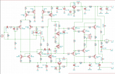
1st image: original schematic (LDA192)
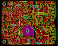
2nd image: board layout (LDA192)
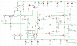
3rd image: newer schematic (LDA192-1)
The changes in the new schematic affect three things:
- the Bias spreader is different
- the capacitance multipliers are replaced with RC filters
- oscillation reduction on negative clipping [a VA transistor collector to GND capacitor (Cx) and increasing VA transistor emitter resistor (R19)]
So some components had to be removed or short circuited, and Cx (in the VAS) and Rx (in the Bias spreader) had to be installed.
Attachments
Last edited:
I had removed the current mirror temporarily for a quick measurement, and then put it back. Don't worry.
You miscalculated something. The voltage across the 5k6 resistor is about 7V, that means 1.25mA. The bottom of the oscillation envelope is at about 18V. 18/5k6= 3.2mA is the peak collector current during the oscillation.
I stand corrected on the amounts of collector current however the peak emitter current of Q7 will be a similar amount to 3.2 mA - so you might consider the current gain of Q9.
To look at this another way the transconductance of a small signal transistor is about 40 m.A. per volt.
I recommend you re-run the oscillation test and see what the base-emitter voltage is for Q9.
gerenis69
Whether it helps or not, I would increase the value of R19 to 27-30 ohms. With a single ended VAS there is a balancing act of currents from Q7, R14, R19 and the CCS. Could you measure the Vbe of Q9 and dc across R14 and R19 at idle?
Mad
I've already increased R19 to 33 Ohms for a try and it does reduce the oscillation by about 50%. I can't measure distortion, but the sim shows that increasing R19 leads to higher distortion at all frequencies. So I must decide which is more important: a more stable clipping or a lower non-clipped signal distortion.
U R14=795mV
U R19=141mV
Ube Q9=795-141=654mV
measuring stability of the amp
Yes, to confirm what I have kept on saying that the amp is sufficiently stable at around 1MHz ULGF, I tried to make the Miller cap (C5)/ LTP degen resistors (R5,R9) lower to see where the signs of instability occur. I also changed TMC to TPC because TMC has somewhat higher ULGF than Miller comp (MC) with the same C5, R5, R9 values, while TPC has the same ULGF as MC. Capacitive loads were 15nF, 100nF, 2.2uF. I also placed a 4.7pF cap across the 15k feedback resistor (R16) to improve the phase above 2MHz.
Results for TPC (ULGF was taken from LTSpice sim):
R5,R9=150R C5=47pF -> ULGF=0.7MHz, amp stable with all capacitive loads
R5,R9=150R C5=33pF -> ULGF=1.1MHz, amp stable with all capacitive loads, clipping behaviour somewhat worsens
R5,R9=100R C5=33pF -> ULGF=1.8MHz, amp stable with all capacitive loads, though clipping bahaviour gets worse, especially with 15nF load
So I'm convinced that if the amp is still stable at 1.8MHz with all kind of capacitive loads, then it can take 0.7MHz or 1MHZ happily...
The ringing freq at clipping is always very close to 1MHz independently of where the ULGF is. This also confirms to me that the ringing on clipping is not due to loop instability but something else. Like a parasitic oscillator formed somewhere?
But I don't like the idea of making a 10V lower rail to -VCC. Instead making the VA transistor into a cascode could be easier and cheaper, so then I could use a low voltage transistor for VA, which I suppose works better at low Vce than KSC3503. (Wonder if the KSC3503 is to blame for not being blameless enough?") )
)
The PCB traces from the rail decoupling caps to the OPT collectors span about 7-9cm (2.7"-3.5"). I wanted get them closer when I designed the PCB but couldn't find an easy way to do that, so they remained a bit too distant. Could it be the problem?
I've now simulated a version of your design, which confirms that it is stable with TMC compensation.
Yes, to confirm what I have kept on saying that the amp is sufficiently stable at around 1MHz ULGF, I tried to make the Miller cap (C5)/ LTP degen resistors (R5,R9) lower to see where the signs of instability occur. I also changed TMC to TPC because TMC has somewhat higher ULGF than Miller comp (MC) with the same C5, R5, R9 values, while TPC has the same ULGF as MC. Capacitive loads were 15nF, 100nF, 2.2uF. I also placed a 4.7pF cap across the 15k feedback resistor (R16) to improve the phase above 2MHz.
Results for TPC (ULGF was taken from LTSpice sim):
R5,R9=150R C5=47pF -> ULGF=0.7MHz, amp stable with all capacitive loads
R5,R9=150R C5=33pF -> ULGF=1.1MHz, amp stable with all capacitive loads, clipping behaviour somewhat worsens
R5,R9=100R C5=33pF -> ULGF=1.8MHz, amp stable with all capacitive loads, though clipping bahaviour gets worse, especially with 15nF load
So I'm convinced that if the amp is still stable at 1.8MHz with all kind of capacitive loads, then it can take 0.7MHz or 1MHZ happily...
The ringing freq at clipping is always very close to 1MHz independently of where the ULGF is. This also confirms to me that the ringing on clipping is not due to loop instability but something else. Like a parasitic oscillator formed somewhere?
But I don't like the idea of making a 10V lower rail to -VCC. Instead making the VA transistor into a cascode could be easier and cheaper, so then I could use a low voltage transistor for VA, which I suppose works better at low Vce than KSC3503. (Wonder if the KSC3503 is to blame for not being blameless enough?
)The PCB traces from the rail decoupling caps to the OPT collectors span about 7-9cm (2.7"-3.5"). I wanted get them closer when I designed the PCB but couldn't find an easy way to do that, so they remained a bit too distant. Could it be the problem?
Oh, I forgot: The above stability tests were done with resistor R17 increased from 2k74 to 4k7. It's more a cosmetic change than having any significant effect (except for improving phase margin a little bit like 5 degrees or so), but to me the amp sounded better with the higher value R17.
When listening, I always tend to hear more difference between MC and TPC, and only a little difference of what the actual compensation (ULG Freq) is. With TMC or TPC I feel like I hear more detail but also exaggerated high harmonics in the range where the ear is most sensitive, which is disturbing to me. With MC it sound more natural but with less detailedness. How much is psychology and how much is a real difference? Hard to tell. Although I told you before that this amp sounds much less "edgy" with MC, I'm not sure if I could tell which compensation is which on a blind listenig test...
When listening, I always tend to hear more difference between MC and TPC, and only a little difference of what the actual compensation (ULG Freq) is. With TMC or TPC I feel like I hear more detail but also exaggerated high harmonics in the range where the ear is most sensitive, which is disturbing to me. With MC it sound more natural but with less detailedness. How much is psychology and how much is a real difference? Hard to tell. Although I told you before that this amp sounds much less "edgy" with MC, I'm not sure if I could tell which compensation is which on a blind listenig test...
Last edited:
There is no output protection for this circuit - one hopes the driver base resistors - value 22R are not wire wound types. While 100R film types might work in a simulation 220R is more likely to prevent damage during the time it takes for rail fuses to blow.
I have protection on a different board, which I soldered up just yestrday and haven't tested yet. This thread is not about protection circuits, so I didn't mention it. All low wattage resistors are 0.6W metal film.
Last edited:
So is R19 33 or 20 ohms, with 141mv? You don't want Q7 effecting the CCS current through Q9 very much. If you don't want to short R13 you need a cap across it, with R13 the current gain of Q7 is much lower.
Mad
R19 is 20 ohms, with 141mV across it.
Sim shows that the loop gain is 101dB at low frequencies. When I short R13 in the sim it goes to 102dB. So the current gain seems to be high enough even with the reduction caused by the 5k6 collector resistor.
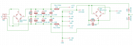
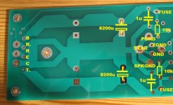
Will you guys pls review my PS layout? Maybe the connection of the 1u caps is not ideal, and the STAR point is having some unwanted HF ripple?
For clarity, I omitted the Loudspeaker SSR from the schematic of the PS, and cut off is the right side of the pcb so the Ground Loop Breaker and SSR part is not visible.
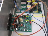
(Note that the picture of the amp was taken a long time ago when the cap-muls were still in place and Cx had not been fitted yet.)
For clarity, I omitted the Loudspeaker SSR from the schematic of the PS, and cut off is the right side of the pcb so the Ground Loop Breaker and SSR part is not visible.
(Note that the picture of the amp was taken a long time ago when the cap-muls were still in place and Cx had not been fitted yet.)
Attachments
Last edited:
I still suggest you try connecting the negative rails together (current mirror and VAS supply to the - rail). (Without the 0.68 ohm and cap mag, not even an RC filter).
Simulations have shown that an unwanted impedance in the lead between the VAS neg supply and neg supply might induce the oscillations of the sort you are seeing. I had to use larger inductances than I would expect for capacitors, but simulators tend to ignore magnetic coupling between tracks.
Some use a high frequency gain reducing RC network across the base of the first stage of the VAS (I still think of this as a Darlington device and an emitter follower where the signal is taken from the emitter. In this instance the first of the VAS pair is just used as a current amplifier.) such as 470pF and then the same resistor as used in the emitter of the VAS transistor. Typically I use 22 ohms for both. The capacitor could be increased to 1nF. Distortion will increase at the upper audio band but that might not be noticably so in reality. This provides a gain reduction with a corrected phase shift at high frequencies.
I've already increased R19 to 33 Ohms for a try and it does reduce the oscillation by about 50%. I can't measure distortion, but the sim shows that increasing R19 leads to higher distortion at all frequencies. So I must decide which is more important: a more stable clipping or a lower non-clipped signal distortion.
U R14=795mV
U R19=141mV
Ube Q9=795-141=654mV
Q9 looks OK and R19 should not be increased however you are going on about parasitic effects without having paid any heed to the messages in posts 58 and 59.
You should note that the equivalent to Q7 in Self's blameless has the collector connected directly to earth. Also note the use of 100R stopper resistors in the driver stage these are to prevent sticking effects under overload conditions. The effects of sticking will be worse in a higher power amplifier.
The way things are heading there are some things you will have to learn the hard way.
Last edited:
More comparisons with Self
@gerenis69
I have looked at a simulation for Self's Invariant amplifier - which is similar to his Blameless - this for the want of someone posting a simulation of this present circuit.
In the Invariant, the equivalent to Q7 has an emitter resistor of 2.2k the same value I suggested recently. A point of difference in comparison to the present circuit is that the equivalent of Q7 connects to earth.
Anyway I ran the Invariant simulation - to a peak voltage out of 34 V into 4R.
The peak Q7 collector and emitter currents were between 400uA and 570uA and the peak base current for Q9 equivalent is 54-144 uA.
You have a 5.6k resistor interposed between Q7 collector and earth with a peak current of 3.2 mA across it.
I mentioned in the earlier post that there is a diffusion capacitance between the collector and base of Q7 which is inversely proportionate to the square root of voltage applied to the collector.
You seem to have changed some values in direct proportions to those used by Self - you cannot cover impacts that arise in inverse proportions by that means.
You have doubled the emitter values for the current mirror transistors over the values used by Self and increased the LTP transistor emitters to match.
The capacitance developed across the collector to base diffusion will look like a capacitor across Q7 input.
This impact is avoided in the Invariant circuit since the collector is at zero volts. In the circumstances you may like to reflect on the departures from Self's circuit.
You should note that the equivalent to Q7 in Self's blameless has the collector connected directly to earth. Also note the use of 100R stopper resistors in the driver stage these are to prevent sticking effects under overload conditions.
The problem I see with this approach is twofold. First, there is no current limit in the VAS transistor. Therefore the current will be limited only by the base current into the emitter follower of the pair and the VAS transistor, which could be rather high. That may be enough to destroy the VAS.
The second problem is more subtle. The 100 ohm limiting resistor in the base of the driver transistor(s) should in principle limit the current, but this could be almost 400mA! But if the current exceeds about 70mA the NPN driver transistor reverse base voltage could be exceeded, which will cause that to conduct and that may be destroyed.
I have not seen many references to this potential hazard, but the original Blameless had no protections anyway. Presumably because any standard protection circuit would increase distortion.
For this reason I recommend a series resistor in the collector of the emitter follower transistor, bypassed with a small capacitor, rather than series base resistors to limit the current. However, the absence of a resistor means that the emitter follower transistor runs with the highest possible collector voltage, more or less constant, and therefore with lowest distortion due to Early effect. The resistor therefore needs to be as low as possible consistent with current limiting. I would also recommend a passive (e.g. two or three diode string) to limit the current in the VAS, depending on the emitter resistor), as any protection on the base of the emitter follower could well introduce significant distortion (more sensitive part of the circuit).
However, the 100 ohm base resistors also affect the frequency response and though I have not analysed this it may contribute to stability. Bailey used 100 ohm resistors in his 1968 design, apparently for short circuit protection reasons. One reason I suggest that they may not be necessary is that I never found this to make a difference in a Bailey design in practice, in stability terms, whereas attention to decoupling, grounding did.
Last edited:
The problem I see with this approach is twofold. First, there is no current limit in the VAS transistor. Therefore the current will be limited only by the base current into the emitter follower of the pair and the VAS transistor, which could be rather high. That may be enough to destroy the VAS.
The second problem is more subtle. The 100 ohm limiting resistor in the base of the driver transistor(s) should in principle limit the current, but this could be almost 400mA! But if the current exceeds about 70mA the NPN driver transistor reverse base voltage could be exceeded, which will cause that to conduct and that may be destroyed.
I have not seen many references to this potential hazard, but the original Blameless had no protections anyway. Presumably because any standard protection circuit would increase distortion.
For this reason I recommend a series resistor in the collector of the emitter follower transistor, bypassed with a small capacitor, rather than series base resistors to limit the current. However, the absence of a resistor means that the emitter follower transistor runs with the highest possible collector voltage, more or less constant, and therefore with lowest distortion due to Early effect. The resistor therefore needs to be as low as possible consistent with current limiting. I would also recommend a passive (e.g. two or three diode string) to limit the current in the VAS, depending on the emitter resistor), as any protection on the base of the emitter follower could well introduce significant distortion (more sensitive part of the circuit).
However, the 100 ohm base resistors also affect the frequency response and though I have not analysed this it may contribute to stability. Bailey used 100 ohm resistors in his 1968 design, apparently for short circuit protection reasons. One reason I suggest that they may not be necessary is that I never found this to make a difference in a Bailey design in practice, in stability terms, whereas attention to decoupling, grounding did.
I was over dramatic with comments about following the Self design more closely. This was more about the resistor values than structure of the circuit.
If the values of R13 and R14 are increased the disparity in currents in Q7 as compared with Self's circuit can be corrected with some allowance for the fact the present circuit has to deliver 200W into 4R.
I suggested a value of 2.2k for R13 but none for R14 which might be in 10 k multiples. The value selected will have an impact on the Miller capacitance between Q7 collector to base -hence the need for a capacitor in parallel with R14 on which we agree.
- Status
- This old topic is closed. If you want to reopen this topic, contact a moderator using the "Report Post" button.
- Home
- Amplifiers
- Solid State
- Help! Oscillation and "rail override" problem with my power amp