R13 is important to limit the current/dissipation in both the Darlington VAS transistors!
Try the capacitor first.
Then consider using higher supply rails for the pre-stages rather than a passive cap-mag filter. If you saturate the OP stage before the VAS it could stop your oscillation problem, but you will need to find a way to limit the VAS current.
Rather than a transistor current limiter I suggest a passive diode string (three diodes with a voltage drop of ~1.8V and an emitter resistor in the VAS of 22 ohms should provide 30mA max. limit. Maybe the KSC can handle that, needs checking too.)
R13 is important to limit the current/dissipation in both the Darlington VAS transistors!
Try the capacitor first.
My intent was to focus on the whole Vas area which in my view has some unwitting changes.
In the light of these a 1nF capacitor in parallel with R13 is only a first step.
As I see it the first thing needing attention is the question of the Vas being driven into saturation - this possibility raised in post 2 by Mark Johnson.
To deal with this the value of R14 has to be considered and the selected value of 680R is plainly too low from the viewpoint of drive current to the Vas.
Furthermore increasing the current increases the amplification factor of Q7. Due to the Miller effect the collector to base capacitance will be greatly increased.
There will be slew rate consequences arising out of this and in the absence of a parallel bleed capacitor around R13 the slew rates will be uneven.
I think D2 should be deleted and R13 will need to be increased to get the tuning of Miller capacitance to the right level where there is harmony with a 1nF capacitor in parallel.
As I see this there has been some adaption of an original circuit (or circuits) and it is time to reflect on what these have been.
Last edited:
Just to coment that I finished to build a second version of my experimental amp this time with CCS loaded VAS (not bootstrap as the first) and again I got the dreaded oscillation on the negative peaks, even with zobel outside the board...I diid a couple of tricks then a gave up and went to "simple" cascoded common emitter VAS: amp is stable and sounds good. I use 3.2mA per side on the input "pair".
I will implement Hawksford cascode tomorrow and see if that improves sound.
The base of the cascodying element must be around 3.2V above (-) rail given my experience and Self's book. I guess this comes with early clipping but it is alright for me as I don't need much power.
I hope this helps.
M
I will implement Hawksford cascode tomorrow and see if that improves sound.
The base of the cascodying element must be around 3.2V above (-) rail given my experience and Self's book. I guess this comes with early clipping but it is alright for me as I don't need much power.
I hope this helps.
M
I think D2 should be deleted and R13 will need to be increased to get the tuning of Miller capacitance to the right level where there is harmony with a 1nF capacitor in parallel.
R13 should be chosen to limit the current to the VAS, in my view. "Tuning" does not really apply to a CR network, the purpose of the capacitor is to simply keep the collector of the first of the VAS pair at a low impedance to eliminate Miller effect -at least at high frequencies to improve the frequency response- as much as possible and the value is probably not critical.
R13 should be chosen to limit the current to the VAS, in my view. "Tuning" does not really apply to a CR network, the purpose of the capacitor is to simply keep the collector of the first of the VAS pair at a low impedance to eliminate Miller effect -at least at high frequencies to improve the frequency response- as much as possible and the value is probably not critical.
I said this since Q8 will develop Miller capacitance which will need to be driven from the emitter of Q7 which has a collector load and it's own Miller capacitance.
In a sense Q7 is a phase splitter and there appears to be a design intent to have this work more in push-pull to improve the drive symmetry - this by balancing the collector and emitter loads including the elements of capacitance.
If push - pull is possible the standing current of Q7 could be reduced.
A 1nF capacitor in parallel might be enough if the right value for R14 (and R13) can be found.
Thank you all who advised me. I have been busy for a few days but now I'm back, and I'm gonna look at your advices.
The following changes have been made relative to my original schematic so far:
D4 shorted
D5 shorted
R21 changed to 1k6
Rx (2k7) installed between B of Q11 and B-C of Q12
Cx (470p) installed between collector of Q9 and GND
R19 changed to 20R
R43 changed to 10R
Also decided to remove the two capacitance multipliers because they behave very nastily as soon as the difference between the ripple on the HT rail and the average voltage on the HT rail comes near or exceeds the built in voltage drop of the cap-muls. So I had to choose whether to omit them or make them drop a much bigger voltage. I decide to remove them and use only simple RC filters. The associated changes:
Q13 removed
D6 removed
R24 removed
R25 changed to 47R
C8 top end connected to where Q13 Emitter was
Q16 removed
D7 removed
R28 removed
R30 changed to 47R
C12 top end connected to where Q16 Emitter was
So here is how the schematic stands currently (see attached image).
Attachments
As suggested by R Dijk in post 29 to resolve this situation the current mirror emitter resistors need to be reduced in value.
Reduced them to 47R, but not the slightest change is visible in the clipping behaviour.
I chose the value of 150R, which is higher than 68R in the original Blameless amp, because my amp was meant to be a 200W one, so it has higher closed loop gain than the 50W Blameless, and noise considerations come into play.
A further improvement
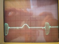
I use an old Onkyo chassis to house this prototype amp. So it came handy to use of one of its speaker terminals with its little PCB that had a 10nF cap across the speaker hot and ground. I totally forgot about this little cap thinking that 10nF is too small to cause any problem. Simulation showed that the most "dangerous" capacitive load to bring the amp into oscillation is about 100nF.
When I removed this 10nF cap, the oscialltion amplitude was further reduced from about 3V p-p to about 1V p-p now.
However the sound of the amp didn't change. It was just as "edgy" as it had been before. Then I removed the TMC resistor R17 to make the amp into "normal" Miller compensation. I did this a few times during testing, and saw nothing different on the oscilloscope with or without TMC. Miller comp. shows the same oscillation on clippping. But have never listened to the amp with normal Miller comp. Well, now I did: the sound is very different: much more natural, with much less "edginess".
If this is a 200 W amplifier into 4R the supply rails would have to be around the 60 volt mark. The changes you made to the CCS suggest an operating current around 7 m.a.
Run a test using the same settings that induced the 1 V p-p anomaly you reported but this time monitor the voltage at the collector of Q7 with respect to earth and advise the result.
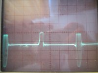
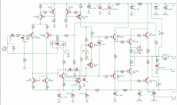
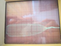
Sorry, the first image in my previous post was 5V 50us...
Here are two other images, this time I removed the LTP current mirror and instead placed a 820 Ohm collector load onto the input transistor. Same measurement (Q7 collector): First image 5V 50us, second image 5V 5us.
Here are two other images, this time I removed the LTP current mirror and instead placed a 820 Ohm collector load onto the input transistor. Same measurement (Q7 collector): First image 5V 50us, second image 5V 5us.
Attachments
Tried, no change.I would suggest that, if you have not already done so, omit (short) the "base stopper" resistors in the OP transistors (2.2 ohms) and drivers (22 ohms).
Tried 1 uF and no change. In fact LTSpice shows that significant cross conduction through the OPTs occurs only above at 30kHz. Is there any other reason for this cap? I can't decrease the 68 Ohms, the drivers are on a separate small heatsink, and it can't take more heat.Then, reduce the base-base resistor between the output stages (68 ohms =>33 ohms) and add a 1 ... 10 uF capacitor as mentioned before.
Can you suggest a better trasnsitor instead of KSC3503?While the spec's of the KSC3503 look good, I suspect the low Cjc is due to a lightly doped collector measured at 30V. Two consequences are (1) the lightly doped collector may impact the fT quite seriously at low collector voltages (<10 or perhaps 5V) and (2) the capacitance will increase. Both effects will make the phase shifts worse near negative clipping.
Yes, it's about the same. With TMC and TPC, the oscillation is a little bit higher when the signal is coming out of clipping.Also, you show the design using TMC compensation. Does the oscillation still occur if you use standard Miller?
The ULGF is about 0.9MHz with TMC, about 0.7MHz with Miller and with TPC (with 150Ohm and 47pF). This doesn't seem to me to too high with these fast transistors. Simulation shows stability problems only below 15pF. As far as I know open loop unity gain really doesn't play any role, it's the Unity Loop Gain that matters for stability. This amp has a closed loop gain (Acl) of 31, much higher than the Acl of 20 of the original Blameless design. (And the amp is stable into different capacitive loads, it's only the negative clipping that provokes the oscillation.)For 10Mhz unity gain bandwidth and 150 ohm LTP resistors, the Miller capacitor needed would be 100pF: 47 pF equates to 20MHz which would be more sensitive to layout (trace inductances, power supply to PCB trace (unintended magnetic couplin g) effects. So try 100pF in addition to the other mods.
They were simple cap-muls, no supply below -VCC. I'd like to avoid making the whole amp more complex than necessary. I've already removed even the cap-muls and replaced them with simple RC filters.I also note that you have a stabilised supply for the input stages. -As I can't see the circuit while writing this I'm not sure if it is lower than the - rail. If not, it may help to make it 10V below the neg rail to offset the higher capacitance/quasi-saturation resistance of the high collector epi mentioned, but you may then need to clamp the swing to the neg rail.
Last edited:
Sorry, the first image in my previous post was 5V 50us...
Here are two other images, this time I removed the LTP current mirror and instead placed a 820 Ohm collector load onto the input transistor. Same measurement (Q7 collector): First image 5V 50us, second image 5V 5us.
Don't try changes to other areas.
From the voltage drop across R13 (5.6K) there is 8.9 ma flowing from the collector of Q7 through this component.
The amount of collector current in a transistor depends on the gain but for arguments sake lets say 99% of the emitter current ( for a transistor with the % equates to the current gain divided by the current gain plus one).
Accordingly you have about 9 m.a. of emitter current available from Q7 to drive Q9 base which is causing Q9 to saturate. To remedy this the values of R14 and R13 have to be increased in value.
If you want see that you are on the right track in the first instance increase the value of R14 to 2.2k and re-run the tests.
I've now simulated a version of your design, which confirms that it is stable with TMC compensation. Suggests that we are looking for a parasitic component in the output stage. I now wonder about your rail stabilisation policy. I've seen negative rail oscillations on quasi OP stages when epi base transistors are used which can be suppressed with usually 220pF from VAS collector to ground or the collector connection to the PNP driver, but this is largely due to the phase shifts in the PNP/NPN which are well known to be less stable than PNP/PNP stages.
I wonder if the capacitors you are using are low impedance at high frequencies, and maybe feeding the output stage ripple into the ground causing unexpected feedback.
To test this I'd try omitting the 0.68 resistors and connecting C13 and C15 to the power ground, not the GNDA. (and in the positive rail if this works, but I'm convinced its an unexpected coupling in the OP stage wiring).
Contrary to what I suggested before, if it is a local parasitic then increasing the resistor in series with the base of the PNP driver might help (e.g. 100 ohms), but it may be better to review the wiring layout and consider cross coupling and grounding schemes first.
Last edited:
I assume that the decoupling capacitors C15, C16, C17, C19 are on the PCB next to the OP transistors? I have seen oscillations due to power supply wiring (as mentioned 50 years ago by Bailey) being longer than about 4 inches without decoupling. That oscillation was fixed too by grounding the local decoupling capacitors with a short wire too.
One more thought... I mentioned before that I recommend the VAS stage to be operated from a LOWER voltage than the - supply to the OPS. Just to test this, try shorting the pass transistor/capacitor multiplier at see if tying the VAS and input stage - rail to the - supply stops the oscillation. Again check where the ground leads to these are routed. I'd keep the VAS decoupling capacitors in the supply line, but take the GNDS to PWRgnd.
But could you define GND , GNDA and GNDPWR?
Any impedance between the VAS emitter feeding into the input (by some means) may cause the oscillation.
But could you define GND , GNDA and GNDPWR?
Any impedance between the VAS emitter feeding into the input (by some means) may cause the oscillation.
Sorry ... to answer your questions:
absence of base stoppers makes my point they aren't needed, even if it did not help!
I try to choose the base resistor and capacitor combo to avoid charging as much as possible to the bandwidth of the amp, which in most cases is higher than 30kHz, but I agree 30kHz may be adequate for some less stringent demands.
The KSC3503 looks a good transistor, but the DS shows the fT at 30V. It might be a lot lower at 5V or near saturation, which most models won't show as they don't account for quasi-resistance. (VBIC model does but even now is not very commonly available compared with SPICE). I'd use it with a lower rail voltage as mentioned.
Stability is about the phase shift and gain over frequency, so high open loop UG freq helps to design a higher closed loop UG bandwidth. But in your case I think we are looking for a parasitic.
And your last point, I now suspect it could be the negative rail (de)coupling/impedance causing the problem. TO add to my previous reply, if you short out the filter transistor connect all the decoupling caps to GNDPWR and see if that works.
Haven't investigated with LtSpice but it's probably worth to note what the current mirror is doing during clipping.
Negative clipping: the bias to the mirror is lost because the back side LTP transistor cuts off, causing both mirror transistors to cut off. All the 3 mA tail current is dumped through the front side LTP transistor, clamping diode, and the VAS transistor.
Positive clipping: front side LTP transistor cuts off but back side LTP transistor remains conducting. The bias to the mirror is never lost. Both mirror transistors remain conducting, although the bias side transistor gets all the tail current less base current to the "business" side transistor, while the latter stays in saturation due to collector current starvation.
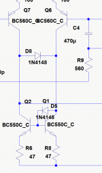
I have seen similar amp circuits having a diode across the current mirror transistor collectors that I suspect was for the purpose of keeping the mirror from cutting off during negative clipping. D8 in the attached pic would keep the mirror conducting and sharing the tail current during negative clipping.
I'd wonder if that diode could make a difference to the oscillation mechanism or hopefully a cure.
I might add that care should be taken of the bias circuit of the current mirror to ensure the cross diode never conducts during normal operating conditions.
Just a thought.
Negative clipping: the bias to the mirror is lost because the back side LTP transistor cuts off, causing both mirror transistors to cut off. All the 3 mA tail current is dumped through the front side LTP transistor, clamping diode, and the VAS transistor.
Positive clipping: front side LTP transistor cuts off but back side LTP transistor remains conducting. The bias to the mirror is never lost. Both mirror transistors remain conducting, although the bias side transistor gets all the tail current less base current to the "business" side transistor, while the latter stays in saturation due to collector current starvation.
I have seen similar amp circuits having a diode across the current mirror transistor collectors that I suspect was for the purpose of keeping the mirror from cutting off during negative clipping. D8 in the attached pic would keep the mirror conducting and sharing the tail current during negative clipping.
I'd wonder if that diode could make a difference to the oscillation mechanism or hopefully a cure.
I might add that care should be taken of the bias circuit of the current mirror to ensure the cross diode never conducts during normal operating conditions.
Just a thought.
Attachments
- Status
- This old topic is closed. If you want to reopen this topic, contact a moderator using the "Report Post" button.
- Home
- Amplifiers
- Solid State
- Help! Oscillation and "rail override" problem with my power amp