The previous circuit prevent the CE voltage of Q2 from falling during a positive clip, and then having a delay as it rises again, leaving Q3,Q4 in the off condition delaying the output coming off clipping. Rail sticking etc happens when early stages overdrive past clipping etc, so you need diodes or something to stop them going beyond that point. Any point connected to a compensation capacitor or other capacitance can not be allowed to wander outside the linear region since it takes time to pull them back. The same applies to internal transistor capacitance but that small capacitance only causes problems in very fast circuits. This is another reason that large feedback loops are so problematic.
This post is kind of OT ... or at least off to the side and not a solution to the solution as it is manifesting itself. It's an observation. Treat it as you will
Going back many years, the one thing I was taught was to keep it simple. It was considered easier to make an output stage able to handle more power that you want, and then to apply any signal limiting to prevent the output stage fromentering limiting to prevent these strange states.
Far easier to control the drive TO the output stage than to control the behaviour of the output stage when you drive it to limiting. As steveu points out, it's important to keep devices in their linear regions. A 75 watt amp is going to behave a lot better than a 50W amp when driven to 50W output!
Now by all means, tell me to go away!!!")
Going back many years, the one thing I was taught was to keep it simple. It was considered easier to make an output stage able to handle more power that you want, and then to apply any signal limiting to prevent the output stage fromentering limiting to prevent these strange states.
Far easier to control the drive TO the output stage than to control the behaviour of the output stage when you drive it to limiting. As steveu points out, it's important to keep devices in their linear regions. A 75 watt amp is going to behave a lot better than a 50W amp when driven to 50W output!
Now by all means, tell me to go away!!!
Hi Generis69,
Can you post an updated schematic?
Have you tried base stopper resistors on your CCS transistors?
Best wishes,
M.
The most recent circuit is attached to post 68 which shows this has been done. It also introduces a lag capacitor to the output of the Vas Cx 470 pF.
This is worse than superflous since it introduces yet another pole making the in-fighting such than none of them has enough domination.
Re stopper resistors I would increase the values of those in the output transistors bases - there are notches in the latest 'scope pictures which suggest output stage sticking effects.
This post is kind of OT ... or at least off to the side and not a solution to the solution as it is manifesting itself. It's an observation. Treat it as you will
Going back many years, the one thing I was taught was to keep it simple. It was considered easier to make an output stage able to handle more power that you want, and then to apply any signal limiting to prevent the output stage fromentering limiting to prevent these strange states.
Far easier to control the drive TO the output stage than to control the behaviour of the output stage when you drive it to limiting. As steveu points out, it's important to keep devices in their linear regions. A 75 watt amp is going to behave a lot better than a 50W amp when driven to 50W output!
Now by all means, tell me to go away!!!
I agree with all that you have said in this post.
Have you tried increasing the power supply rails to the pre-stages rather than having a voltage drop in the filter sections you originally showed?
No, I haven't. I don't want to make the amp overly complicated if not strictly necessary. I think I can do with a bit of oscillation on clipping. I just don't want that big surge current during positive rail sticking.
Some time ago I removed the 100u-47R RC filter from the positive rail to the IPS-VAS as somebody recommended, but unfortunately I haven't reported on that for you guys. Sorry, I update the schematic now.
Ry1 and Ry2 at the input of the beta enhancer (Q7) is only experimental and probably won't remain. I just played with them to reduce the Loop Gain (LG) at low frequencies from 100dB to about 80dB without upsetting the current mirror balance too much. I know D. Self suggests a resistor between the VAS C and B to to this, but that resistor -- if too low -- upsets the VAS biasing and causes a peak in the loop gain with two-pole compensation. Putting a big series film capacitor there is not elegant. But I'm not sure that reducing the low freq. LG (and so shifting the -3dB rolloff point of loop gain higher) does any good to sound quality... At least I can't hear any persuasive difference when I listen to music with this lower LG setup.
Attachments
and as mjona points out you should still add a small capacitor across R13, if you have not done so.
No, I haven't done so, but I'd like to. I must decide what type of capacitor and what the exact value should be.
That's not oscillations on the positive clip. It's just a clip level that follows the power supply ripple. If you adjust the sweep to near 120xN, you will see the clip wave up and down as it beats with the supply ripple frequency, or sync to "line"(AC) and you will just see just one clip line.
Yes, you are very probably right. Thank you!
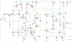
Correct schematic and LTSpice file
There is a mistake in the schematic at post #125. The Jx jumper was put in the wrong place. It's to select between Miller and TPC. Here I upload the correct schematic.
Hi mjona, Without Cx, the "lag" capacitor, negative clipping will become Hell Unleashed. I can't see any problem with the pole introduced by Cx.
Or am I making a mistake in simulation? I upload the LTSpice file, you guys can check the effect of Cx or anything you want. Unfortunately the simulation doesn't show any oscillation problem at clipping, so the KSC3503 model may be very inadequate. Inductances are all parasitic except for L1=1u at the output.
For any difference found between the schematic and "200W LDA192-1.asc" file, the schematic is decisive.
To see the loop gain plot: Run the simulation and Add new trace "-1/(1-1/(2*(I(Vi)@1*V(x)@2-V(x)@1*I(Vi)@2)+V(x)@1+I(Vi)@2))".
To run transient and check THD, set prb to zero. Set freq and/ or input signal level as you like. The THD data is saved in the Spice error log.
Attachments
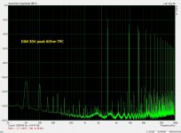
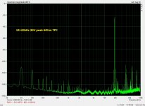
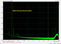
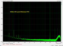
distortion measurements
I could buy an E-MU 1212M PCI card and could do some measurements with ARTA. The E-MU driver (there is no official win7 driver for the PCI version card) throws me a BSOD every single day, but the E-MU card itself is very cheap for its noise and for its 1kHz THD performance and does fine at 192kHz sampling rate.
Surprisingly at 20kHz the E-MU performed worse than the Steinberg UR22 mkII, which I had over from a friend for a couple of days. However at 1kHz the Steinberg had about 10x higher distortion. So all measuremetns were with the E-MU, except the 20kHz was with the Steinberg. (20kHz THD only incorporates 3 harmonics beacuse of the 96kHz limit.)
Measurements were 30V peak signal into 6 Ohm resistive load (about 75 Watts). All measurements turned out to be around the distortion of the sound cards specified in their manuals, or even lower, so the power amp itself probably has lower distortions than measured. It would require a finer equipment to know for sure. DIM is Dynamic InterModulation distortion.
So the prediction of the Spice simulation is good about distortion figures, they are very low.
Attachments
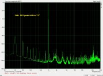
listening impression this time with E-MU 1212M
No matter how low the measured distortion, I don't fully like the sound I hear when I listen to music, although I got used to it over time. It sounds better with the E-MU card, than with the built in soundcard I used before, it's even cleaner and detailed, but I still can distinctively hear some metallic edge on high frequency transients that gets annoying sometimes, especially on high pitched guitar strings, but more static sounds like violins and women's voices also tend to sound "highish" or "thin". Although it varies with recordings, not all recodings sound so, there are many that sound pretty nice, so I don't understand.
My speakers I made myself back in 2003. It has a Visaton G20SC high-end soft dome tweeter in it, so I don't think it's the tweeter, besides I had a few commercial amplifiers since then and don't remember any of them sounded like this. Well I'm very critical of my work, so perhaps it also plays a role in my judgement. I'm not sure I could tell another good amp from this one on a blind test.
Another issue: I usually listened to the same FLAC recordings from Youtube over and over when listening. Just now realized that Youtube converts all lossless uploads like FLAC to youtube's own lossy format, so perhaps I need to find get some original lossless audio files to test with.
There is a mistake in the schematic at post #125. The Jx jumper was put in the wrong place. It's to select between Miller and TPC. Here I upload the correct schematic.
Hi mjona, Without Cx, the "lag" capacitor, negative clipping will become Hell Unleashed. I can't see any problem with the pole introduced by Cx.
Or am I making a mistake in simulation? I upload the LTSpice file, you guys can check the effect of Cx or anything you want. Unfortunately the simulation doesn't show any oscillation problem at clipping, so the KSC3503 model may be very inadequate. Inductances are all parasitic except for L1=1u at the output.
For any difference found between the schematic and "200W LDA192-1.asc" file, the schematic is decisive.
To see the loop gain plot: Run the simulation and Add new trace "-1/(1-1/(2*(I(Vi)@1*V(x)@2-V(x)@1*I(Vi)@2)+V(x)@1+I(Vi)@2))".
To run transient and check THD, set prb to zero. Set freq and/ or input signal level as you like. The THD data is saved in the Spice error log.
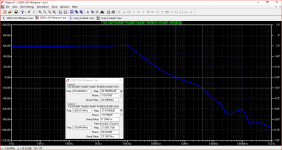
I have looked at this and tried some changes - I am away from home on holiday and I need to do some more checking when I have the time.
I note you have made some allowance for parasitics however I have doubts the circuit would be immune from influence when the phase plot rises as it did in my first simulation. This can be made to trend differently as shown as attached.
I am on holiday and need a bit more time to look at the changes I have made. One of these was to lower the impedance of the feedback system (2.2k/120R)
I did not save my initial simulation where I used some different .models
Attachments
Last edited:
If you have too much gain, just use larger values in the diff-amp emitter resistors (150->220->330). Ry1,2 cause bias problems. You could use 150 +100 Ohms and a jumper between the two sides to select 150 vs 250 per emitter. The (100/2=) 50 in series with the current source is actually a good idea. I know DSelf likes Darlington VAS, but the extra gain puts a stress on stability. A lot of degenerated stages adds a lot of poles. Local degeneration is a great idea if there is no outer feedback loop. You may have noticed that Pass has resorted to super simple two-stage amps.
I did not like the shapes in the phase and gain plots in post 131.
The strategy of adding parasitic elements looks to me like adding complexity which could be a two edged sword.
Unless such effects can be modelled reliance on covering these should rest on adequate phase and gain margins.
The strategy of adding parasitic elements looks to me like adding complexity which could be a two edged sword.
Unless such effects can be modelled reliance on covering these should rest on adequate phase and gain margins.
Another Possible Approach
My simulation is attached. The gain and phase margins are reduced in this version and the unity gain point is at roughly half the frequency in the original.
In the natural world phase alters more quickly than gain will decline. It is possible in a simulation to boost phase so there is a delay causing this to lag behind to some extent.
I have included the expression which needs to be pasted in the vout header as a comment in blue on the .asc file. The .models are all due to Cordell and the .inc statement is linked to his website.
For this version the trend in decline reaches an early point where the plots run in parallel. There is no secondary boost in the phase. If you look at post 131 it can been seen how irregular the shape of the second boost was and see perhaps why I did not like it.
The low pass input and output zobel filters are out of circuit - there is little difference with this engaged in the circuit.
I have run THD tests at 20 kHz the results don't match the comments in blue which refer to the downloaded version. This is about 0.01% however I felt the FFT pattern was not as good as might have been hoped.
This might be useful for comparative purposes
Attachments
Last edited:
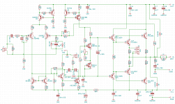
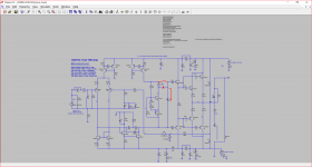
This partial schematic illustrates a way to avoid positive rail sticking.
I have tried the circuit you proposed in post #119. Unfortunately it didn't stop the rail sticking nor the current surge across the output transistors. The LTSpice simulation also showed that the current mirror transistor does go into saturation, and your circuit prevents it. (The simulation also showed however that the current mirror transistor leaves this saturated state very-very quickly, so it doesn't really affect rail sticking.) Perhaps that is why this method doesn't work with my amp. The "significant" saturation occurs somewhere else.
However I could decrease the current shoot-through across the output transistors to a level where the overcurrent protection doesn't encroach, by adding a speedup capacitor across R29. Both you and John Ellis proposed this capacitor before, but at that time I didn't install it because both the LTSpice simulation and the datasheet suggest that the OPTs are fast enough to prevent significant shoot-through even at a 30kHz full swing signal. Well maybe they are fast enough to prevent cross conduction around zero crossing but maybe not fast enough near the positive rail at low Vce.
The optimal value of this capacitor still needs to be found, because if it's too big, then it does more harm than it does good.
Last edited:
I have tried the circuit you proposed in post #119. Unfortunately it didn't stop the rail sticking nor the current surge across the output transistors. The LTSpice simulation also showed that the current mirror transistor does go into saturation, and your circuit prevents it. (The simulation also showed however that the current mirror transistor leaves this saturated state very-very quickly, so it doesn't really affect rail sticking.) Perhaps that is why this method doesn't work with my amp. The "significant" saturation occurs somewhere else.
However I could decrease the current shoot-through across the output transistors to a level where the overcurrent protection doesn't encroach, by adding a speedup capacitor across R29. Both you and John Ellis proposed this capacitor before, but at that time I didn't install it because both the LTSpice simulation and the datasheet suggest that the OPTs are fast enough to prevent significant shoot-through even at a 30kHz full swing signal. Well maybe they are fast enough to prevent cross conduction around zero crossing but maybe not fast enough near the positive rail at low Vce.
The optimal value of this capacitor still needs to be found, because if it's too big, then it does more harm than it does good.
The first thought that comes to mind is what impact are the output transistor stopper resistors having on the speed up capacitor across R29 and considering there are 100R base stoppers in the driver stage are these 2.2 ones strictly necessary.
An additional thought about the problem with the positive swing relates to the connections for R7 in the Vbe circuit.
The way the Vbe is configured has R7 in series with R16 while R7 forms a low pass filter in combination with C1 - see attached.
The collector of Q16 should connect directly to R16 stopper resistor and to collector Q8 via R7.
For checking purposes see the attached image.
The way the Vbe is configured has R7 in series with R16 while R7 forms a low pass filter in combination with C1 - see attached.
The collector of Q16 should connect directly to R16 stopper resistor and to collector Q8 via R7.
For checking purposes see the attached image.
Attachments
Attached is a simulation for a peak output voltage just over 40 volts giving a THD of about 0.017% into 8R at 20kHz. The FFT looks tidier than in an earlier simulation I ran. Apart from the change in the location of R7 and altering the Vbe bias in consequence, I reduced the value of R30 in the simulation from 150k to 100k.
It may be worth testing other values by simulation and look at the damping resistor R4 value and the values of C6 and C4 as well.
I did not find any improvement from a speed up capacitor across R8 in the simulation and it was an arbitrary decision to omit the 2.2R stopper resistors.
I have not matched the part numbers in the simulation to the original file it might be useful to tidy up this detail when your work is complete. Treat this simulation as indicative only.
Attachments
- Status
- This old topic is closed. If you want to reopen this topic, contact a moderator using the "Report Post" button.
- Home
- Amplifiers
- Solid State
- Help! Oscillation and "rail override" problem with my power amp