A simple check to try , it might get us closer . With the amp off for at least 10 mins connect your multimeter directly across the left hand output terminals and measure the resistance , you should see approx 2300 ohms ( continuity all the way through to the feedback network ) . You can obviously compare it with the other channel .
There are a lot of red wires connecting the heat sink assembly to the pcb check each red wire is going to the correct pcb pad , include the green ground wire .
There are a lot of red wires connecting the heat sink assembly to the pcb check each red wire is going to the correct pcb pad , include the green ground wire .
The three 0.1's (C15, C21 and C23) would not cause this problem. If C15 was open circuit then the amp might be unstable but the scope is saying no.
The 33pF. I'd have to say no for the simple reason that even if one of them were faulty (leaky or short circuit), you would still have the 1.28 volts applied to the other one and that FET pair would work normally.
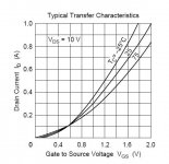
I've changed a simulation I had of a lateral FET amp to match your output stage. This is what you should be seeing. Do you see how the FET gates draw no current. There is no volt drop across the 220 ohms. The voltage between the 220 ohms should be identical at the left and right sides (your 1.28 volts). That kind of voltage causes around 200ma to flow in the lateral FET's. You should be seeing similar to this on each parallel pair of FET's.
(Ignore the 33pF on the lower FET as the designer hasn't fitted them on the lower P channel FET's.)
Thanks for mocking this up. The only part I'm having trouble following (and perhaps indicates I've been taking these measurements incorrectly) is the bolded part. I had interpreted "between the 220 ohms" to mean the voltage between the two 220 ohm resistors connecting the K135 gates (and then between the two 220 ohm resistors linking the J50 gates).
A simple check to try , it might get us closer . With the amp off for at least 10 mins connect your multimeter directly across the left hand output terminals and measure the resistance , you should see approx 2300 ohms ( continuity all the way through to the feedback network ) . You can obviously compare it with the other channel .
There are a lot of red wires connecting the heat sink assembly to the pcb check each red wire is going to the correct pcb pad , include the green ground wire .
So the right (good) channel does measure exactly 2300 ohms. The left channel measures 2000 ohms.
Looking back at measurements in post 1 it appears that the right channel has a similar problem, but at least one pairs working.
Gate voltages indicates that it should draw current in some way but the 6V (!) Means full on wich would give full rail on output, but it isn't.
The low values across source resistors indicates that no current flows, that they are broken, or that the fets don't conduct.
I would have checked all fets and it's wiring first.
Then source resistors, they might be broken when higher current flows.
And I'm still suspicious about those sockets
Figge
There used to be a good schematic along with a manual of sorts that was on a Russian website, can’t find it now however...
In 1984, Erno Borbely published a two-part series of articles on the DC 100, and its related Servo 100, in Audio Amateur. I have hard copies and can make pdf's out of them if you like. I'll send it via PM.
The DC 100 is similar to the Hafler DH220 driver boards, which uses similar Hitachi MOSFETS. I have the Hafler, and it is prone to "loss of bias" (the MOSFETS) stop drawing current). As I recall, there was a broken driver transistor.
The DH220 draws about 270 mA across the output MOSFETS, similar to the DC 100.
Regarding broken MOSFETS, the Hitachi's are pretty tough, and on the DC 100, the set of diodes between the two MOSFET gates (D11 to D14) protect the MOSFET gates from over-voltage. See if the zener, especially, is broken. This could be a hint for problems at the MOSFETS. There are some quick tests for broken MOSFETS using a meter and low voltage supply - see Nelson Pass's site.
So the right (good) channel does measure exactly 2300 ohms. The left channel measures 2000 ohms.
Can you repeat the measurements maintaining the same polarity for each channel and then do the same with reversed polarity for both channels .
Can you repeat the measurements maintaining the same polarity for each channel and then do the same with reversed polarity for both channels .
LEFT: 2000 ohms
RIGHT: 2200 ohms
LEFT (Rev. polarity): 1600 ohms and rising
RIGHT (Rev. polarity): 700 ohms and rising
Regarding broken MOSFETS, the Hitachi's are pretty tough, and on the DC 100, the set of diodes between the two MOSFET gates (D11 to D14) protect the MOSFET gates from over-voltage. See if the zener, especially, is broken. This could be a hint for problems at the MOSFETS. There are some quick tests for broken MOSFETS using a meter and low voltage supply - see Nelson Pass's site.
Thanks for directing me toward the FET testing info at Nelson Pass's site. Re the diodes D11 to D14, I replaced them last week. I just checked them again, and they're good.
Thanks for mocking this up. The only part I'm having trouble following (and perhaps indicates I've been taking these measurements incorrectly) is the bolded part. I had interpreted "between the 220 ohms" to mean the voltage between the two 220 ohm resistors connecting the K135 gates (and then between the two 220 ohm resistors linking the J50 gates).
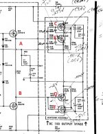
I've marked on the diagram to illustrate.
Also attached is the transfer characteristic of a typical 2SK type lateral FET. You can see how it begins to conduct at relatively low gate/source voltages. The 2SJ type is similar except that the gate voltage is negative with respect to the source.
So your measure 1.28 (was it?) volts across the 150 ohm should be getting the FET's nice and hot.
Looking back at measurements in post 1 it appears that the right channel has a similar problem, but at least one pairs working.
Gate voltages indicates that it should draw current in some way but the 6V (!) Means full on wich would give full rail on output, but it isn't.
The low values across source resistors indicates that no current flows, that they are broken, or that the fets don't conduct.
I would have checked all fets and it's wiring first.
Then source resistors, they might be broken when higher current flows.
And I'm still suspicious about those sockets
Figge
Its an odd result for sure. And if a gate was floating then I think the FET would just start to conduct heavily as the gate 'floated' its way to some undefined voltage.
Attachments
Of course, now that you indicated the points to measure (C and D), it seems obvious. Where's the head slapping emoji when you need it?
I'll redo the measurements.
Regarding potentially swapping transistors around, it appears that the owner/builder of this amp soldered the pins to the sockets. First time I've encountered this. Typical?
I'll redo the measurements.
Regarding potentially swapping transistors around, it appears that the owner/builder of this amp soldered the pins to the sockets. First time I've encountered this. Typical?
No problem
Soldering to T03 sockets probably isn't typical but stranger things have happened.
New measurements:
Across the 150 ohm resistor (between A and B): +1.27V
Across the top FET's 220 ohm resistors (C and D): +0.77V
Across the bottom FET's 220 ohm resistors (C and D): +1.27V
The low figure for the top FET's does include that J50 with the green socket.
I also input a 1kHz sine wave and checked with my scope to see if it was present at the gates of the output transistors. It was.
Last edited:
Hmmm ")
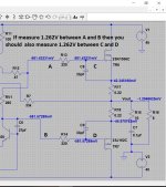
1.27 across the 150 ohm is fine. That is A and B.
Look at the diagram attached.
Between C and D should be 1.27v
Between E and F should be 1.27v
Between C and F should also be 1.27v
Between E and D should also be 1.27v
There should be NO voltage between C and E and no voltage between D and F
The sine wave you applied as a test. Did you also see that sine wave at the junction of the 0.22 ohms ?
Attachments
Hmmm
1.27 across the 150 ohm is fine. That is A and B.
Look at the diagram attached.
Between C and D should be 1.27v
Between E and F should be 1.27v
Between C and F should also be 1.27v
Between E and D should also be 1.27v
There should be NO voltage between C and E and no voltage between D and F
The sine wave you applied as a test. Did you also see that sine wave at the junction of the 0.22 ohms ?
Morning coffee followed by morning measurements:
Between A and B: 1.23V
Between C and D: 0.77V
Between E and F: 1.23V
Between C and F: 1.23V
Between E and D: 0.75V
Between C and E: 0V
Between D and F: 0.46V
Re the sine wave, yes I picked it up at the junction of the 0.22 ohm resistors.
Well this is getting interesting...
First question (which ignores all the voltage measurements). If you can pick up audio (the sine wave) on the 0.22 ohms, then you should be able to hear that via the speaker.
The readings. Hmmm, These just don't add up tbh and the readings involving the lower FET's seem screwy. We have to carry on with this line of attack though.
It appears that the upper FET's are giving reasonable results, both C and E have no voltage difference between them and also C to F and E to F both maintain the 1.23v.
So that leaves FET 'D' as seeming to give weird results.
What to do next.
The sine wave that you can pick up on the junction of the 0.22 ohms should also be present on the + speaker terminal. Check that it is.
Does adding a speaker as a load 'kill' this sine wave voltage or can you hear the sine test tone. (Keep the amplitude of the tone to a couple of volts peak to peak). The amplitude should not change at all as a load (speaker) is added.
If the speaker kills the voltage then we have to consider that the FET's are faulty in some totally weird kind of failure mode.
First question (which ignores all the voltage measurements). If you can pick up audio (the sine wave) on the 0.22 ohms, then you should be able to hear that via the speaker.
The readings. Hmmm
, These just don't add up tbh and the readings involving the lower FET's seem screwy. We have to carry on with this line of attack though.It appears that the upper FET's are giving reasonable results, both C and E have no voltage difference between them and also C to F and E to F both maintain the 1.23v.
So that leaves FET 'D' as seeming to give weird results.
What to do next.
The sine wave that you can pick up on the junction of the 0.22 ohms should also be present on the + speaker terminal. Check that it is.
Does adding a speaker as a load 'kill' this sine wave voltage or can you hear the sine test tone. (Keep the amplitude of the tone to a couple of volts peak to peak). The amplitude should not change at all as a load (speaker) is added.
If the speaker kills the voltage then we have to consider that the FET's are faulty in some totally weird kind of failure mode.
- Status
- This old topic is closed. If you want to reopen this topic, contact a moderator using the "Report Post" button.
- Home
- Amplifiers
- Solid State
- Borbely DC 100 Amp: Left Channel Troubleshooting