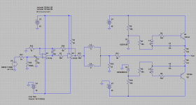
I have been reading an article regarding Nelson's F6 amplifier, and I really liked the idea of using a transformer to drive the output voltage followers. Out of many amplifier designs, this was the one I could really understand well. This, and a pair of LL1527 transformers lying around gave me an idea to try building an new amp. But this time with "my" design ") .
.
What I didn't like with F6 was the pair of matched JFETs that make the input buffer. You just cannot find these, yet alone matched. Thus idea of using an op amp was born. Obviously not a new one, but I was quite happy with it.
Next was to choose output devices. Since this was to be "my" design, and I always wanted to build something with Darlington transistors, the choice was to use Audio Darlington pair from Sanken, the STD02N and STD02P. However, since you cannot find PSPICE model for these, for first run in LTSPICE, quick Google search led me to TIP141/TIP146. By no mean remarkable, but it allowed me to play around with it.
Since I was using LTSPICE, it was logical to use LT's op amp. Looking through datasheets, I found a schematic for a buffer with LT1010 buffer and LT1056 op amp. I though that LT1115 would be a better choice than LT1056, and the final schematic was born.
Now the funny thing. After some playing around with feedback resistors and Zener voltage (there will be a pot there for calibration like with F6 in the final design, I was too lazy to put one in now), I got some nice transfer function and calculated THD 0.005%.
Then I got an idea to replace the output transistors with some "better" audio ones, like MJL4302A/MJL4281A. But the resulting THD was not better than 0.04%. I also tried many other On Semi's Darlingtion pairs, but in any case the result was the same.
What am I doing wrong? How come TIP141/TIP146 can have best results?
Also, is there anything you think can be improved with the schematic?
.What I didn't like with F6 was the pair of matched JFETs that make the input buffer. You just cannot find these, yet alone matched. Thus idea of using an op amp was born. Obviously not a new one, but I was quite happy with it.
Next was to choose output devices. Since this was to be "my" design, and I always wanted to build something with Darlington transistors, the choice was to use Audio Darlington pair from Sanken, the STD02N and STD02P. However, since you cannot find PSPICE model for these, for first run in LTSPICE, quick Google search led me to TIP141/TIP146. By no mean remarkable, but it allowed me to play around with it.
Since I was using LTSPICE, it was logical to use LT's op amp. Looking through datasheets, I found a schematic for a buffer with LT1010 buffer and LT1056 op amp. I though that LT1115 would be a better choice than LT1056, and the final schematic was born.
Now the funny thing. After some playing around with feedback resistors and Zener voltage (there will be a pot there for calibration like with F6 in the final design, I was too lazy to put one in now), I got some nice transfer function and calculated THD 0.005%.
Then I got an idea to replace the output transistors with some "better" audio ones, like MJL4302A/MJL4281A. But the resulting THD was not better than 0.04%. I also tried many other On Semi's Darlingtion pairs, but in any case the result was the same.
What am I doing wrong? How come TIP141/TIP146 can have best results?
Also, is there anything you think can be improved with the schematic?
Attachments
With the F6, the output fets create all of the voltage gain as well as the current to drive the speaker. That is why the input stage is just a buffer for the line level input. Your circuit is simply a opamp gain stage driving transistors with a transformer thrown in that doesn't really do anything.
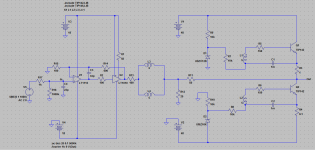
OK, so since the consensus is that complementary pair has no sense in this circuit, I've made a version with TIP142 used for both output devices. New schematic attached.
Could it be that the results of the simulation are better with TIP142 vs the MJL4281A, is lower base current?
Also what do you think the purpose of that 1 MOhm resistor in the input is? I copied it from the data sheet, but not really sure why it is there.
Thank you all for your help.
Could it be that the results of the simulation are better with TIP142 vs the MJL4281A, is lower base current?
Also what do you think the purpose of that 1 MOhm resistor in the input is? I copied it from the data sheet, but not really sure why it is there.
Thank you all for your help.
Attachments
The U2 is a buffer, essentially just to boost current capacity, therefore only one input. And you can make global feedback as its gain is set to 1.
And since I cannot edit my previous post, let me rephrase my question so that it is clear Is the reason that TIP141 work better than MJL4281A in the simulation because of lesser base current?
Anybody have any idea about that 1 megaohm resistor at the input?
And since I cannot edit my previous post, let me rephrase my question so that it is clear
Is the reason that TIP141 work better than MJL4281A in the simulation because of lesser base current?Anybody have any idea about that 1 megaohm resistor at the input?
R16 is normally about 47k.
D1 & D2 should be the same.
R3 & R4 should be the same.
I would take simulated THD with a pinch of salt because the transistor models are of variable accuracy. I would take THD with a pinch of salt anyway. Being able to use same polarity output devices is a benefit of using a transformer.
D1 & D2 should be the same.
R3 & R4 should be the same.
I would take simulated THD with a pinch of salt because the transistor models are of variable accuracy. I would take THD with a pinch of salt anyway. Being able to use same polarity output devices is a benefit of using a transformer.
The D1, D2, C1, C2 biasing system looks a bit suspect to me. I'm not sure what Nelson Pass was thinking here. The biasing is not Identical for the two output devices. Zeners are noisy and ought to be muffled by some caps.
Also bear in mind that this scheme was designed for mosfets which have very different bias requirements from bipolars. Double-check that it works properly.
Also bear in mind that this scheme was designed for mosfets which have very different bias requirements from bipolars. Double-check that it works properly.
I was planning to move to the topic of the Zener diodes later. I have also been reading about how noisy they are, that is the reason why in F6 blue LED is used. I was thinking about one of those Zener replacements such as AD780.
Regarding the C1 and C2, what Mr. Pass said while presenting F6 at Burning Amp festival in San Francisco in 2012, is: To see to it that the secondary still presents a low AC source impedance to the Gate of the transistor, we couple it to the Source pin through large value capacitors C1 and C2.My understanding of this is simple logic that output impedance of the previous stage should be low.
As for the values of the D1 and D2, in final version there will be pots in parallel to them (or their replacement) that will be used for adjusting the output current (bottom one) and DC offset (upper one). I have been playing with Zener voltages instead, and the funny combination shown in last schematic is the result of playing around with the simulation.
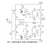
For R3 and R4, at the above mentioned conference, Mr. Pass said that their values affect second and third harmonic, respectively. There was even a version of F6 where impact of these could be adjusted via a pair of pots, as given attached. He suggested that these can be used to improve distortion, and change the character of the output sound (more second or more third harmonic). I have been playing with the values for R3 and R4, and for values from my last schematic I got least THD (arguable if at all relevant, but interesting).
Thank you for your help.
Regarding the C1 and C2, what Mr. Pass said while presenting F6 at Burning Amp festival in San Francisco in 2012, is: To see to it that the secondary still presents a low AC source impedance to the Gate of the transistor, we couple it to the Source pin through large value capacitors C1 and C2.My understanding of this is simple logic that output impedance of the previous stage should be low.
As for the values of the D1 and D2, in final version there will be pots in parallel to them (or their replacement) that will be used for adjusting the output current (bottom one) and DC offset (upper one). I have been playing with Zener voltages instead, and the funny combination shown in last schematic is the result of playing around with the simulation.
For R3 and R4, at the above mentioned conference, Mr. Pass said that their values affect second and third harmonic, respectively. There was even a version of F6 where impact of these could be adjusted via a pair of pots, as given attached. He suggested that these can be used to improve distortion, and change the character of the output sound (more second or more third harmonic). I have been playing with the values for R3 and R4, and for values from my last schematic I got least THD (arguable if at all relevant, but interesting).
Thank you for your help.
Attachments
Most likely then I am doing something wrong, just I am not sure what
Maybe the truth is that the TIP141/142 model has some flaw that, in combination with emitter resistor misbalance creates this illusion of really low THD. That would also explain why MJL4281A model has 15x higher THD in the simulation, although I expected an improvement.
The final F6 schematic has top resistor 0.56 and bottom resistor 0.47. Would you consider this to be good practical boundary for difference between the two emitter resistors?
Also what would be good NPN Darlington for this amplifier? Would 2SD2560 be a good choice?
I think this is an interesting circuit for you to play around with. I think the First Watt F6 has limitations and seems to be an exercise in simplicity over function. But do pursue what you are trying because you will learn something.
Note that you are using bipolars (eventually darlingtons) rather than MOSFETs and their drive characteristics are radically different. You should consider these differences carefully and examine whether the drive circuit is still optimum. Or you can just build it and see what happens.
Also ask yourself why should the emitter resistors be different values at all?
This indeed is supposed to be a learning journey for me. I definitely want to build this, but I wanted to ask for opinion of more experienced designers. My electronics education was more focused on analysis of the circuit, rather than design.
What I see in the schematic are two class A amplifier, top one in common collector configuration, and the bottom one in common emitter configuration. As such, their amplification is completely different, as common collector amplification can be approximated to be 1 with Darlington (BF > 1000), where the amplification of common emitter is BF*Rb/Rc, where Rb is equivalent resistance as seen by transistor base and Rc equivalent resistance as seen as transistors collector. Given this, it is not entirely impossible to me that you could indeed have different resistors R3 and R4.
The problem is that the simulation shows, even when TIP142 is replaced with BDV65B, that THD goes down when R3 > R4. Since this could be the error of the simulator, as you have pointed out, my only solution is to narrow it down to two options:
- make top 0.56 and bottom 0.47 as in F6
- make both 0.47 ohm (better than both 0.56 in the simulation)
Now if I finalize R3 and R4 to 0.47, BDV65B does give better results than TIP142, that I expected.
Furthermore, I have discovered that when Darlington is substituted with MJL4281A (normal NPN), the THD goes up a bit, but more interesting is its collector current. Any ideas why would this be like this?
In comparison, BDV65B gives normal sine curve, although THD in both cases is almost the same (0.03 vs 0.025).
Attachments
Yes an no. Yes at dc. No at ac. Imagine C1 & C2 being short circuits at ac. This is what makes the dc bias arrangement different between the two.What I see in the schematic are two class A amplifier, top one in common collector configuration, and the bottom one in common emitter configuration.
What is more interesting about its collector current?Furthermore, I have discovered that when Darlington is substituted with MJL4281A (normal NPN), the THD goes up a bit, but more interesting is its collector current. Any ideas why would this be like this?
You need to keep the dc current through R3 & R4 about the same between sims.
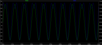
I find it odd that the AC current has two peaks, one just before and one just after the peak of the output voltage. Since it is running in class A, I expected current to have same waveform as the output voltage.
The DC current through R3 and R4 is almost the same, some needs to go to the feedback circuit.
Speaking of which, should bathe resistors in the feedback loop be larger values, to reduce DC current going to the transformer primary?
The DC current through R3 and R4 is almost the same, some needs to go to the feedback circuit.
Speaking of which, should bathe resistors in the feedback loop be larger values, to reduce DC current going to the transformer primary?
Which ac current are you referring to? An image of the waveforms would help.
If you adjust D1 for zero dc offset at the output then there should be negligible current flowing through the primaries.
What I meant was that you want the dc current flowing through the output transistors (the class A bias) to be a certain target value. When you change transistor types you want to make sure the current is adjusted close to that value or your comparisons will be messed up.
- Status
- This old topic is closed. If you want to reopen this topic, contact a moderator using the "Report Post" button.
- Home
- Amplifiers
- Solid State
- Frankenstein amp