Some thinking questions for you ")
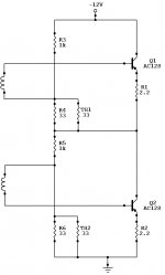
1. What is unusual about the negative feedback of the F6? How does it differ in its frequency characteristics from a conventional loop, like you would see around an op-amp?
2. And can you therefore explain why the Q1 dc bias circuit is different in its connections to that of Q2?
3. Can you suggest another way of keeping the output dc offset near zero AND making the current bias of each output transistor use the same circuit topology?
Would you please show the plot of V(out), I(R3) and Ic(Q4)?
I have plotted Ic(Q2), I assume that is what you wanted to see. I tried to match the steady state current for both BDV65B and MJL4281A as much as possible. Maybe I should have put batteries instead of the Zener diodes to be able to adjust this better.
Anyhow the waveform for BDV65B looks more what I expected.
Attachments
I have found this two MOSFET schematic for a buffer that I liked, therefore I replaced the op amp in the input with it. I find the fact it is AC coupled complements the design of the power stage. The simulation results are not as great as with op amp, but I find this much more interesting.
The buffer design is based on "triodizator" circuit that is supposed to emulate behavior of a triode. I thought it would be interesting to hear how it sounds.
The voltage follower and the power supply are taken from a design of Fetishizator (I prefer Fetizator), another design I have always considered interesting.
There is a tread in Analog Line Level where this design was proposed and is discussed. I would post a link to it if I knew how to do it. Subject is Help analyze the circuit. I did quick simulation of it and decided to add it to my design.
Please let me know if you see anything that should be corrected.
Attachments
As I am now preparing to build this, please help me with selection of components. My only option for buying components are Digikey and Mouser, and shipping to me from USA is quite expensive. All in all, I would like to avoid making multiple orders I am quite confident about most of the components, but I need help with few.
I have already asked about the output transistors, is it OK to go with BDV65B or there are better NPN Darlingtons out there. Somehow I always considered Sanken a good choice for BJTs, what do you think? How many of these do you think is required to be ordered to get them decently paired.
Also, the input cap and the one at the input of transformer are critical. I had Elna Silmic electrolytes in the output stage of my DAC, that were simply horrible. The biggest upgrade was removing them. Therefore I will be using film capacitors. Any objections? Since the supply voltage for the input section is +/- 20V, I guess 63VDC ones should be fine?
Also while routing the PCB, I guess I should have a separate ground planes for the input section and output section. I saw some designs where these two are connected with 10R resistor, but never fully understood why. Is this recommended? What I learned in school was to put ground on whole bottom of the PCB, but none of my classes were about making audio circuits
Thank you all for your help.
I am quite confident about most of the components, but I need help with few.I have already asked about the output transistors, is it OK to go with BDV65B or there are better NPN Darlingtons out there. Somehow I always considered Sanken a good choice for BJTs, what do you think? How many of these do you think is required to be ordered to get them decently paired.
Also, the input cap and the one at the input of transformer are critical. I had Elna Silmic electrolytes in the output stage of my DAC, that were simply horrible. The biggest upgrade was removing them. Therefore I will be using film capacitors. Any objections? Since the supply voltage for the input section is +/- 20V, I guess 63VDC ones should be fine?
Also while routing the PCB, I guess I should have a separate ground planes for the input section and output section. I saw some designs where these two are connected with 10R resistor, but never fully understood why. Is this recommended? What I learned in school was to put ground on whole bottom of the PCB, but none of my classes were about making audio circuits
Thank you all for your help.
I can't say. I never use darlingtons. You might also consider buying a pair of IGBTs for experimenting - they have a drive characteristic a little more like a FET.I have already asked about the output transistors, is it OK to go with BDV65B or there are better NPN Darlingtons out there. Somehow I always considered Sanken a good choice for BJTs, what do you think? How many of these do you think is required to be ordered to get them decently paired.
C4 is about 10 times larger than it needs to be. You can therefore use a small size/cost film cap. I like polypropylene. You should use your simulation to meausre the worst case voltage across C5 but I imagine it will only be a few volts. Note that the AC rating of film caps is a lot lower than their DC ratings.Also, the input cap and the one at the input of transformer are critical. I had Elna Silmic electrolytes in the output stage of my DAC, that were simply horrible. The biggest upgrade was removing them. Therefore I will be using film capacitors. Any objections? Since the supply voltage for the input section is +/- 20V, I guess 63VDC ones should be fine?
I never use ground panes. The input gnd should go to your star gnd point separately from the output zobel and speaker return otherwise the common path resistance will cause an error voltage at the input and other nasties. There are several threads here discussing ground paths.Also while routing the PCB, I guess I should have a separate ground planes for the input section and output section. I saw some designs where these two are connected with 10R resistor, but never fully understood why. Is this recommended? What I learned in school was to put ground on whole bottom of the PCB, but none of my classes were about making audio circuits
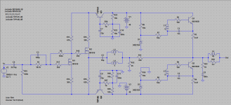
Since I was not so sure about the Darlington transistors, I tried changing the schematic to make the MJL4281A work, but that lead to nowhere. Then it came to me that I could build a Darlington myself using two discrete transistors. The I remembered a schematic from one of Rod Elliott's power amps, and the v2 Frankenstein amp was born. I also tried replacing the current amplification stage made of M2 with a diamond buffer, but that ended up being worse, hence I went back to current gain stage using M2.
In order to eliminate any problems with the power supply, I have decided to run everything on +/- 40V, as IRF610 can withstand Vds of 200V. Because of this I have placed 3 source transistors in order to make them dissipate less than 3W. The value of the equivalent source resistor is also increased in order to reduce the DC current through M2 to a more reasonable level.
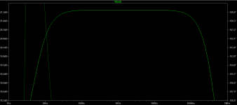
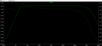
Another change is move of the compensation capacitor from being in series with the M1 input resistor (R19 in this version of the schematic) to connected to the ground. The value have been increased to allow us to remove the Zobel network at the output. Resulting 3dB pass-band and transfer function are attached.
In this configuration I get THD 0.017% @ 35W/8ohm load, way better than with Darlingtons. Of course, real results will be different, as I am guessing the inductance of the primaries/secondaries of LL1527XL.
If you see anything that could be done better, please share
In order to eliminate any problems with the power supply, I have decided to run everything on +/- 40V, as IRF610 can withstand Vds of 200V. Because of this I have placed 3 source transistors in order to make them dissipate less than 3W. The value of the equivalent source resistor is also increased in order to reduce the DC current through M2 to a more reasonable level.
Another change is move of the compensation capacitor from being in series with the M1 input resistor (R19 in this version of the schematic) to connected to the ground. The value have been increased to allow us to remove the Zobel network at the output. Resulting 3dB pass-band and transfer function are attached.
In this configuration I get THD 0.017% @ 35W/8ohm load, way better than with Darlingtons. Of course, real results will be different, as I am guessing the inductance of the primaries/secondaries of LL1527XL.
If you see anything that could be done better, please share
Attachments
- Status
- This old topic is closed. If you want to reopen this topic, contact a moderator using the "Report Post" button.
- Home
- Amplifiers
- Solid State
- Frankenstein amp