Just managed to get hold of some VFETs for my surround room project. I scored 100 used VMP21's (4W, 60V, 1.5A, TO-39) and 95 new KP901A's which are the Russian equivalent of the VMP1 (20W, 70V, 4A, stud-mount).
My last design used the venerable 2SK1058/2SJ162 JFET pair in a 35 watt complementary Class A zero NFB configuration with DC servo and I was very pleased with the way they sounded and measured. Silicon Chip magazine was kind enough to run one through their analyzer and showed them to be flat to 150kHz with acceptable noise figures. Don't ask me to find the results sheet, I haven't seen it in 10 years although I know it's around somewhere.
Anyhow, with all the fuss about VFETs on here I became inspired to try them out. The surround speakers - which are also currently in development - use a Jordan JX125NG with a HiVi RT1C-A ribbon. So, having thought it over, I'll build the first pair with passive crossovers then use the resultant curves to go to the next step, which will be bi-amped using the 4W parts for the tweeters.
There will probably be a passive preamp along the lines of GeorgeHifi's Lightspeed attenuator, but with a bunch of line inputs. Might as well support another Aussie designer.")
I'm not so much of a video nut, in fact I don't even own a television. However, with the surround material available on DVD-A and SACD it seems like a good idea to have at least 5.1 available, and this setup also allows me to monitor the Ambisonic recordings I plan to make with a soundfield mic which is also in development.
In case you think I'm biting off a lot at once, I should point out that I recently retired and these are projects that have been on the backburner for years, so most of the thinking and research stage is over.
Rob
My last design used the venerable 2SK1058/2SJ162 JFET pair in a 35 watt complementary Class A zero NFB configuration with DC servo and I was very pleased with the way they sounded and measured. Silicon Chip magazine was kind enough to run one through their analyzer and showed them to be flat to 150kHz with acceptable noise figures. Don't ask me to find the results sheet, I haven't seen it in 10 years although I know it's around somewhere.
Anyhow, with all the fuss about VFETs on here I became inspired to try them out. The surround speakers - which are also currently in development - use a Jordan JX125NG with a HiVi RT1C-A ribbon. So, having thought it over, I'll build the first pair with passive crossovers then use the resultant curves to go to the next step, which will be bi-amped using the 4W parts for the tweeters.
There will probably be a passive preamp along the lines of GeorgeHifi's Lightspeed attenuator, but with a bunch of line inputs. Might as well support another Aussie designer.
I'm not so much of a video nut, in fact I don't even own a television. However, with the surround material available on DVD-A and SACD it seems like a good idea to have at least 5.1 available, and this setup also allows me to monitor the Ambisonic recordings I plan to make with a soundfield mic which is also in development.
In case you think I'm biting off a lot at once, I should point out that I recently retired and these are projects that have been on the backburner for years, so most of the thinking and research stage is over.
Rob
Last edited:
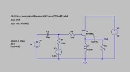
I've made a bit of a start on this. The circuit below shows a tweeter amplifier capable of delivering almost 8W from 1kHz upwards. Distortion figures are:
1kHz:
37mW @ 0.056% distortion - 2.0V p-p in
146mW @ 0.09% distortion - 4.0V p-p in
9W @ 1% distortion - 24.2V p-p in
5kHz:
37mW @ 0.019% distortion - 2.0V p-p in
146mW @ 0.03% distortion - 4.0V p-p in
8W @ 1% distortion - 22.7V p-p in
10kHz:
37mW @ 0.017% distortion - 2.0V p-p in
146mW @ 0.030% distortion - 4.0V p-p in
7.8W @ 1% distortion - 22.4V p-p in
100kHz:
37mW @ 0.026% distortion - 2V p-p in
146mW @ 0.033% distortion - 4V p-p in
7.7W @ 1% distortion - 22.2V p-p in
It's 3dB down at about 1.5MHz so should have enough bandwidth to give toobs a run for their money. Current through L1 is set for 1A and the winding resistance is assumed to be 0.5 ohms.
Attachments
These are being run as followers ?
I always found it hard to distinguish between Fets and vfets in follower mode. I suspect that this is because they behave much the same in this configuration - you have the devices already so I’m sure you’ll find the best use for these exotic beasts - good luck !!.
I always found it hard to distinguish between Fets and vfets in follower mode. I suspect that this is because they behave much the same in this configuration - you have the devices already so I’m sure you’ll find the best use for these exotic beasts - good luck !!.
ilimzn: I just re-read that article in ETI "Vfets for Everyone" and checked the data sheet, and was disappointed to find that in fact the Siliconix VMP series is a V-channel MOSFET and not a VFET/SIT. You are correct, their characteristic is the same as a pentode. Most disappointed because I was hoping to hear some of that VFET magic.
Oh well, at least they were cheap. The low input capacitance still makes them very useful, the KP901A is only 100pF.
Oh well, at least they were cheap. The low input capacitance still makes them very useful, the KP901A is only 100pF.
Still, those are some of the most linear VMOS ever made. Unfortunately none of the EU or US companies ever made SITs, at least not for the general public.
That being said, if you have access to ex-USSR semis, they did make a number of interesting FETs, including JFET, VMOS and VFET. Some of the larger VHF JFETs have very low noise figures and are useful for things like MC cartridge preamps in zero-bias mode.
For VFETs, look for KP801, KP802 and KP926
That being said, if you have access to ex-USSR semis, they did make a number of interesting FETs, including JFET, VMOS and VFET. Some of the larger VHF JFETs have very low noise figures and are useful for things like MC cartridge preamps in zero-bias mode.
For VFETs, look for KP801, KP802 and KP926
These are being run as followers ?
I always found it hard to distinguish between Fets and vfets in follower mode. I suspect that this is because they behave much the same in this configuration - you have the devices already so I’m sure you’ll find the best use for these exotic beasts - good luck !!.
Hi kasey,
Actually I don't yet have these parts, they are still in transit. I was hoping to have a circuit to test them in before they arrive. Wish me luck, I think I'm going to need it. Most of my work has been with bipolar transistors and FETs didn't even exist when I did my training so it's a bit of a learning exercise.
That also explains the 807 in my avatar. It was the first device I used in an amplifier. I found an old WWII transmitter at the dump and turned it into music. A bit of a "swords into plowshares" effort.
It comes down to how charge density is modulated in the semiconductor channel. The manufacturing objectives aim almost exclusively at fast switching between two distinct electrical states, where a well-defined, high on-off current ratio is of overwhelming importance, while complex signal handling is a nonissue. These applications constitute parametric irreconcilability. Insufficient frequency response extensively plaguing semiconductor amplifiers is a source of massive signal distortion. The high frequency regime is cumbersome to manage, it requires the gate length to be short that in turn ordinarily requires the gate dielectric to have substantial nonuniformities and to be a big ugly capacitor limiting frequency performance. The geometrical structure of Japanese VFETs differs from that of all other semiconductors. Conductivity is determined by the correlation between two large repulsive electrostatic forces. As the dielectric material, low density covalent (atomically bonded) silicon dioxide is used without epitaxial layer, avoiding the detrimental capacitance formed under reverse bias by the metallic gate, the extending oxide layer and the semiconductor in the unstable, ionic, ferroelectric P-N junction and in the even more metallic, wide band gap Schottky barrier. Instead, appropriate charge excitation is primarily accomplished by the technologically advanced design of the critical gate-source interface intended to reduce electrostatic shielding. The silicon dioxide dielectric layer is located between the gate electrode and the semiconducting layer, which is also located between the source and the drain electrodes. In the absence of distortive P-N junction, the source and drain electrodes are attached directly to the semiconductor that makes up the capacitive channel, the channel length defined by the thin dielectric layer rather than by the semiconducting layer. The electrodes being stacked vertically in separate layers, and the gate not being positioned between the source and drain, it is a true vertical structure. The result is small inter-electrode capacitances, wide operational frequency range, high saturation velocity, low amplification factor, low gate series resistance, high drain-source channel resistance, rigid electronic coupling, smooth transition of electronic states, preciseness and small losses in the signal formation.
 N101N please add some formatting to your posts, the wall of words is very hard to read.
My problem is that the subject matter cannot be properly described and understood within Classical Mechanics. However, the terms are conventionally used in other theories (Quantum Mechanics, Bond Theory, Optics) and are traceable. Thank you for accepting the statement anyway, I am sorry and will try to exercise restraint.
Some paragraphs would help a lot
That's what I meant by the wall of words, there is no break, and it makes it hard to read. I have reformatted your post in the quote below so you can see what I mean. I may not have split it exactly as you would wish to convey, but hopefully that shows you what I mean.
Tony.
That's what I meant by the wall of words, there is no break, and it makes it hard to read. I have reformatted your post in the quote below so you can see what I mean. I may not have split it exactly as you would wish to convey, but hopefully that shows you what I mean.
Tony.
It comes down to how charge density is modulated in the semiconductor channel. The manufacturing objectives aim almost exclusively at fast switching between two distinct electrical states, where a well-defined, high on-off current ratio is of overwhelming importance, while complex signal handling is a nonissue.
These applications constitute parametric irreconcilability. Insufficient frequency response extensively plaguing semiconductor amplifiers is a source of massive signal distortion. The high frequency regime is cumbersome to manage, it requires the gate length to be short that in turn ordinarily requires the gate dielectric to have substantial nonuniformities and to be a big ugly capacitor limiting frequency performance.
The geometrical structure of Japanese VFETs differs from that of all other semiconductors. Conductivity is determined by the correlation between two large repulsive electrostatic forces.
As the dielectric material, low density covalent (atomically bonded) silicon dioxide is used without epitaxial layer, avoiding the detrimental capacitance formed under reverse bias by the metallic gate, the extending oxide layer and the semiconductor in the unstable, ionic, ferroelectric P-N junction and in the even more metallic, wide band gap Schottky barrier.
Instead, appropriate charge excitation is primarily accomplished by the technologically advanced design of the critical gate-source interface intended to reduce electrostatic shielding. The silicon dioxide dielectric layer is located between the gate electrode and the semiconducting layer, which is also located between the source and the drain electrodes.
In the absence of distortive P-N junction, the source and drain electrodes are attached directly to the semiconductor that makes up the capacitive channel, the channel length defined by the thin dielectric layer rather than by the semiconducting layer. The electrodes being stacked vertically in separate layers, and the gate not being positioned between the source and drain, it is a true vertical structure.
The result is small inter-electrode capacitances, wide operational frequency range, high saturation velocity, low amplification factor, low gate series resistance, high drain-source channel resistance, rigid electronic coupling, smooth transition of electronic states, preciseness and small losses in the signal formation.

Standard MOSFET architecture showing numerous muddying layers, contacts and materials.
Inspired by the working principle of electron tube, the technical realization of VFET is indeed a remarkable achievement. Not every device sorted under the hollow label Static Induction Transistor meets the above criteria for membership in the class.
An exposition worth its salt explaining the connection between voltage-current curves and device performance in understandable language is yet to be presented. It is going to be a challenging enterprise.
The one dimensional mathematical term linearity has come to mean low signal distortion. There is nothing linear (proportional) about amplification whatsoever. Current, voltage, conductance designate a static state and become nonsensical in a dynamic context. Consisting of myriads of spontaneous ephemeral changes, a signal is neither current nor voltage.
I-V curves do not say anything about signal transfer. They have practical relevance to a single stationary operating point. The DC level shifts are actuated dynamically, mainly by the load standing in an indeterminable relation. The strong dependence on energy level and temperature randomizes all parameters. The idealized linear graphs on the paper can be considered to be tube-like, but physical performace can scarcely be tube-like. The electromagnetic field produced by vibrations in the highly dispersive, noisy, contaminated crystal lattice is quite unlike the clean, well shielded, low pressure environment produced by thermionic emission.
Frequency range is inversely related to overall energy level as frequency (velocity = distance per time) is inversely related to both charge separation distance and mass density. Due to exponential distributions, velocity drops rapidly with increasing voltage and with increasing current. That is why transistors devoted to voltage amplification are designed to operate at small currents, and that is why transistors conducting a large current exhibit poor frequency response.
The plain mass times velocity in various old and new disguises: E = mv = ma = mv² = IV = mc² = hv
If my memory serves me correctly, Descartes used it, Leibniz used it (in the form mv²) before Newton, also Maxwell and Poincaré used it before Einstein.
It is up to everyone to deem if it denotes impetus, momentum, force, power, work, energy, electricity or something else.
"Readability" is a bug of mine. My Mom was a newspaper editor, trained in the days before tabloid click-bait; Dad was an engineer who worked to put his thinking into words to influence bosses and customers.
I use gut-sense but also tools. I used to have a good suite of text-tools but alas. MS Word (at least my old copy) has "something". It can be exceptionally stupid so you have to see if the counts even make sense. (Note the paragraph counts!)
Flesch Ease is very easy to compute. Flesch-Kincaid Grade is easy and maybe more "accurate" for most texts; it is also scaled to the US school-grades 1-12.
Mom would want 90% of a newspaper to be readable at a 9th-grade level. Not that the readers were all drop-outs; for ease-of-reading.
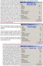
The "It comes down to how charge density is modulated.." post scores as Grade 18, nominally post-graduate college. I have seen higher, but from a bunch of PhDs who were not really saying anything. "Ease" is a low 9. (It may also be "wall of words", and paragraphing helps my eyes, but does not change the computed scores, at least to MS-Word's tiny mind.)
haiqu’s post scores Grade 12, ease 56. This may be quite appropriate for technical matter with many jargon words.
Curious, I hunted for one of Stephen Hawking’s non-pop papers. WOW! Grade 6, Ease 66! It is possible Hawking or his editors "massaged" the text for computed Readability (it was hot stuff at that time), but it does not read as manipulated.
Note particularly the "Passive Sentences" scores. It is IMpossible for a computer to truly know passive from active voice. However there is a trend I agree with. For his murky topic, Hawking is marvelously active-voice. (So is haiqu, but he’s talking about his system and his feelings and thoughts.)
I use gut-sense but also tools. I used to have a good suite of text-tools but alas. MS Word (at least my old copy) has "something". It can be exceptionally stupid so you have to see if the counts even make sense. (Note the paragraph counts!)
Flesch Ease is very easy to compute. Flesch-Kincaid Grade is easy and maybe more "accurate" for most texts; it is also scaled to the US school-grades 1-12.
Mom would want 90% of a newspaper to be readable at a 9th-grade level. Not that the readers were all drop-outs; for ease-of-reading.
The "It comes down to how charge density is modulated.." post scores as Grade 18, nominally post-graduate college. I have seen higher, but from a bunch of PhDs who were not really saying anything. "Ease" is a low 9. (It may also be "wall of words", and paragraphing helps my eyes, but does not change the computed scores, at least to MS-Word's tiny mind.)
haiqu’s post scores Grade 12, ease 56. This may be quite appropriate for technical matter with many jargon words.
Curious, I hunted for one of Stephen Hawking’s non-pop papers. WOW! Grade 6, Ease 66! It is possible Hawking or his editors "massaged" the text for computed Readability (it was hot stuff at that time), but it does not read as manipulated.
Note particularly the "Passive Sentences" scores. It is IMpossible for a computer to truly know passive from active voice. However there is a trend I agree with. For his murky topic, Hawking is marvelously active-voice. (So is haiqu, but he’s talking about his system and his feelings and thoughts.)
Attachments
Last edited:
By the way, the Siliconix VMPXX and 2N665X series are certainly suitable for audio, especially the ones with a higher drain to source resistance and smaller capacitances (lower power handling capability), so I would not feel disappointed.
Not sure why a high D-S resistance would be desirable, except perhaps that this indicates they weren't intended for switching.
Noting that the ones I bought both have small input capacitance, they should be usable. It's a pity I didn't find some with higher power ratings though.
- Status
- This old topic is closed. If you want to reopen this topic, contact a moderator using the "Report Post" button.
- Home
- Amplifiers
- Solid State
- New VFET build