R7 and P2 determine how much current is flowing through the VAS. Normally, it's just a single fixed resistor. In this instance, they added a variable resistor so that they can adjust the VAS current or to tune it to exactly what they want.
The 2N2222 must not be on the heatsink. Actually, it's not required. A normal trimpot will do. The outputs are 2SK1058 and 2SJ162. They are lateral mosfets. No thermal control is necessary.
The 2N2222 must not be on the heatsink. Actually, it's not required. A normal trimpot will do. The outputs are 2SK1058 and 2SJ162. They are lateral mosfets. No thermal control is necessary.
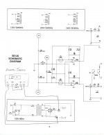
New question. How does the LM393 control the base of Q27 to turn off the current flow when this amplifier gets hot. I know the thermistors are at 10k ohms. They are part number MEPCC#2322-640-63103. The voltages inverting, non inverting and output from the comparators are all negative. This seems like it would keep Q27 turned off all the time and the circuit should not have any current flow through it. Pin 1 of the comparator output is -48.9V and the base of Q27 is -.088 volts. This is what I cannot understand. I have attached the schematic and voltages for this circuit.
Thanks, Mark
Thanks, Mark
Attachments
All, I posted the schematic and voltages from the manual a couple of posts ago. I think somehow Q27 conducts and turns Q9 on or off to stop the amp from overheating. It could also be balancing something between Q5 and Q9 and Q27. I am far from an expert. I know the Q8 and P1 is the VBE multiplier and sets up the drive for Q10 and Q11 to prevent crossover distortion into the mosfet gates and that is only because this forum has provided me the answers and reading some books on my own. I just don't know and am only a small time hobbyist. i sure would like to know so that others with this same amplifier or similar know how to set it P2. Mark
LM393 is a comparator. It compares the two inputs, + and -. When the + input is more positive than the - input the output is open or high. When the -input is more positive than the + input the output will be low. Depending on the circuitry around the comparator the output can be a positive voltage or negative voltage. So under normal conditions the outputs, 1 and 7, will be a high voltage. This high voltage will then bias Q27 on, the base needs to be more positive/ less negative than the emitter. With high temps the + input will get pulled negative because of the thermistors, TS1 and 2, causing the outputs to go more negative turning off Q27 until the temps get back to normal. Is the base less negative than the emitter? Clear as mud now.
Craig
Craig
You do know that you can edit your posts for up to half an hour, right?
All negative? That's a negative. In normal operation at low temperature, LM393 (+in) is maybe 1/3 of the way up between -DCV and VREF. (-in) is only around 10% up at best (hard to say because too many values are unreadable). So then the LM393, being the open collector thingy that it is, would let its output be pulled up to VREF.
With Q27 base being pulled towards VREF, 15 V above -DCV, Q27 turns on hard, much like a switch, and can therefore be treated much like a direct C-E connection.
With rising temperature, the NTC thermistor will reduce its resistance and LM393 (+in) voltage will drop, up to the point where it drops below the constant voltage from the voltage divider at (-in). At this point the comparator will pull its output down, all the way to -DCV. Now the voltage across the 1k - Q27 B-E and diodes CR7-9 is going to be, well, just about zero, or at least no more than 0.2 V or somesuch.
This in turn causes Q27 to stop all this conducting business, and CR7-9 get pinned to -DCV, while CR1-4 get pinned to +DCV. With a reference current of zero, LTP current source Q5 and VAS current source Q8 stop working, and Q6/7 end up pinned against +DCV doing nothing. The bias spreader Q8 has no more current to work with either and reduces its voltage towards zero, bringing down output stage bias to zero as well. Output stage input being pulled to ground via R11 at this point, the output approaches ground potential - not like FETs at zero current are going to do very much pushing or pulling anyway. In short, the amplifier shuts down completely.
The 33k positive feedback resistors on the LM393s provide some hysteria, err, I mean hysteresis. In normal operation, they pull the (+in) voltage up a bit, shifting the threshold up and thus delaying the onset of switching. Once in thermal shutdown, they pull the (+in) voltage down a bit, shifting the threshold down so that the amp has to cool back down a bit before it becomes operational again.
Re: P2, I'm not sure why it's called that, it just sets VAS current. Not sure why this would be adjustable over such a wide range, the probability of a TO-92 like Q8 being run at tens of mA on ~50 V is just about zero (rated Pd typically being 625 mW, so that's 12.5 mA abs max, typically more like 6 mA, maybe less).
Q21 doesn't need to be on the heatsink because that's a lateral MOSFET output stage. Laterals have a negative temperature coefficient so are basically self-stabilizing and don't require thermal tracking like BJTs and most everything else would.
Balance, P2. Best adjusted with a distortion analyzer, but sans that you can adjust it for symmetrical clipping at high signal levels.
Theoretically, you are setting the amp so that it has no offset even without feedback. If P2 were set perfectly (which is not going to happen") ) you could lift the right end of R14 from the output and instead connect it to ground, (opening the feedback loop) and the amplifier offset would remain at zero.
) you could lift the right end of R14 from the output and instead connect it to ground, (opening the feedback loop) and the amplifier offset would remain at zero.
Theoretically, you are setting the amp so that it has no offset even without feedback. If P2 were set perfectly (which is not going to happen
) you could lift the right end of R14 from the output and instead connect it to ground, (opening the feedback loop) and the amplifier offset would remain at zero.All, I do understand your answers and really appreciate your knowledge. I just like to know how these circuits work. I will now try and breadboard the lm393 and try to create a similar on/off trigger event. This helps me learn the behavior of the circuits. I am amazed at the sometimes complicated circuits I see and then when it is explained seems easy. Notice I said seems easy. Thanks, Mark
All on this thread. I am back to experimenting after quite a long time. I think I took too big of a bite. I bought a second Hafler Se120.
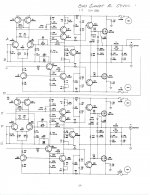
The right channel works, but resistor r53, 30 ohms is burned through and has remained functional. Regardless R53 requires replacement. Question, what caused this resistor to overheat and burn through.
The left channel is not in good shape. R25, 30 ohms and R21, 69 ohms are toasted. R21 is the P Mosfet gate resistor. C14, 100 MFD, 50V, is burned on the side of the can. Both positive and negative rail 4 amp fuses were blown when I opened the amp up amp and I have not replaced them.
Someone replaced the N Mosfet capacitors with 560PF on both channels and they should be 330PF. I cannot tell if these are gate to source or gate to drain.
Lastly, someone replaced the left channel mosfets with 2SK1057/2SJ161 pair, which are a higher voltage rating than the right channel 2SK1056/2SJ160 pair. so at sometime the original pair were blown.
I think someone must have tried to press the stereo/mono switch and blew the fuses, but I am uncertain as to the real mode of failure.
My questions for the DIYAUDIO forum.
1. Can someone please help try and troubleshoot the failure?
2. Does anyone think the output devices are toast, because these mosfets are hard to find and expensives and there are many knock offs from China in the market.
3. I have beginner to sub intermediate soldering skills? The passive components are easy to replace and I can do that work.
4. Does anyone think the 2n5550 and 2n5401 drive pair on the left channel are bad? How would I check them?
5. How far back in the circuit does anyone think the damage goes in the left channel?
6. Does anyone think this is worth repairing? I have minimal money in it right now.
7. Should I replace the passive components and change the 4 amp fuses to something way less and plug it in and try it out? I would pull the right channel rail fuses.
8. Any advice is welcome.
If R53 is burnt, at some point the amplifier behaved very badly, or someone ran high frequency, high amplitude test tones through it. Probably the latter. I think you can replace R53 and be OK. It makes a Zoebel along with C27, to protect the amplifier against loads or speaker cables that might cause instability. Generally, it's most needed when there is nothing connected to the speaker terminals.
If R21 is burnt then Q13 is also gone. Q13 likely emitted its smoke (transistors need to retain their smoke in order to function), and its gate shorted, taking out R21. Q10 is almost certainly also fried. The resulting general DC failure caused there to be too much voltage on C4. I would also check that Q1, Q2, and R13 remain functional. If there was a high enough DC on the base of Q2 to burn out C4, then these components were stressed.
So, I think you may be able to replace Q13, Q10, R21, R25, and C4 and that may be all. Check Q1, Q2, and R13. Do you have a way of bring up the +/- DCV rails slowly, and with limited current? Some kind of bench supply? That would certainly help.
Russell,
Thank you for the help. With Q12 and Q13 gone this makes this a very difficult endeavor. These pairs are hard to find and even the ones listed make it hard to determine legitimate hitachi devices from fakes. While I have okay soldering skills the amount of heat to remove Q12 and 13 may be tedious.
I know I have the skill to replace everything else fairly easily and the parts cannot cost more than $20., with the SK/SJ as the exception.
Why would someone do such a test is beyond me. These are nice performing amps. I was looking for a second one to add to the one I own and use the pair as mono amplifiers.
If R53 is burnt, at some point the amplifier behaved very badly, or someone ran high frequency, high amplitude test tones through it. Probably the latter. I think you can replace R53 and be OK. It makes a Zoebel along with C27, to protect the amplifier against loads or speaker cables that might cause instability. Generally, it's most needed when there is nothing connected to the speaker terminals.
If R21 is burnt then Q13 is also gone. Q13 likely emitted its smoke (transistors need to retain their smoke in order to function), and its gate shorted, taking out R21. Q10 is almost certainly also fried. The resulting general DC failure caused there to be too much voltage on C4. I would also check that Q1, Q2, and R13 remain functional. If there was a high enough DC on the base of Q2 to burn out C4, then these components were stressed.
So, I think you may be able to replace Q13, Q10, R21, R25, and C4 and that may be all. Check Q1, Q2, and R13. Do you have a way of bring up the +/- DCV rails slowly, and with limited current? Some kind of bench supply? That would certainly help.
I do have a precision 0 to 30 volt power supply. I can current limit the supply from microamps to 5 amps. I must ask this question. The power supply has two channels that have positive and negative outputs. I know how to create a true positive and negative voltage for use with op amps. I assume I would do the same thing and then connect the positive to the positive fuse rail for one channel and do the same with the negative lead, but what do I do with the common ground lead? Can I make this plus/minus connection to the output of the rectifier with burning up the rectifier. I would have no AC power line plugged into the wall. I must also power the op amp or the amp will not bias on. I do need to know if this is how you would do this. I cannot get a full 54 volts, but I can get to plus/minus 30 VDC. Do you think this will work? I attached a sketch. Thanks for any advice.
Attachments
- Status
- This old topic is closed. If you want to reopen this topic, contact a moderator using the "Report Post" button.
- Home
- Amplifiers
- Solid State
- Hafler SE 120 Schmatic Explanation