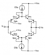
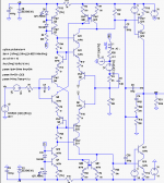
Has anyone seen Rush pairs used this way before? It gives a CFA true-differential inputs.
The circuit below was first posted here
Reasons Of Oscillations In Audio Amplifiers And Best Ways Of Elimination

Normally a CFA input stage has a low input resistance at the inverting input but in this circuit you have a high input resistance inverting input. A CFA can then have true differential inputs with a high CMRR.
The idea is an extension of the Floating OTA Complementary LTP (CLTP) mentioned by Schmid in a 2000 paper linked here (post #2)
Current Feedback Amplifiers, not only a semantic problem ?

I have used this input stage in my Cube-law Class-A amps in Linear Audio Vol.8 and again in Vol.13 (see my sign links for info).
Simulations (attached) suggest you can get 60dB CMRR over the audio range. If you are happy with a lower input resistance on the inverting input then you don't need to add an opamp an the input for a differential-to-single-ended receiver, which is the reason it was suggested for the amp in the above thread. And you can still add DC blocking capacitors to the inputs which lowers the output offset voltage. My example gives 3mV output offset without matching transistors, and 10uF caps gives f-3dB at 15Hz.
For better HF rejection you can add a LPF on each input; split R2 and R10 and add a capacitor from each node to ground (see example in attached zip).
A variant to get a higher input resistance on the inverting input without a high value feedback resistor is attached. It uses a T attenuator for Rf (R9). For 10k input resistance the highest value used is 10K instead of 100k.
There are several down sides with this variant: first, the output offset voltage increases by 10 times. A large capacitor in series with the T ground resistor (~100 ohms) restores the offset to the original ~20mV. The CMRR is about -50dB over the audio range. But you can't add capacitors to the inputs of this variant because the CMRR is then no good at the low frequency end. Maybe someone can find a way to get good CMRR over the full audio range without opmaps.
The mirror transistors (2N2222 & 2N2907) are chosen for their low Is (relative to the BC547/557) for a better mirror ratio of around 10 at idle. The mirror trans-diodes help stabilize the VAS idle current with temperature without sacrificing too much gain and bandwidth.
Lastly, the distortion appears to be mainly from the VAS, probably Early effect nonlinearity, so cascoding the VAS should help reduce the large signal distortion to less than 1ppm in closed loop.
I'm not intending to make an amp using this idea -- I am mainly interested to know if it has been done before, also to let as many as possible know about it since it is so useful for making CFA amps with true differential inputs.
The circuit below was first posted here
Reasons Of Oscillations In Audio Amplifiers And Best Ways Of Elimination
Normally a CFA input stage has a low input resistance at the inverting input but in this circuit you have a high input resistance inverting input. A CFA can then have true differential inputs with a high CMRR.
The idea is an extension of the Floating OTA Complementary LTP (CLTP) mentioned by Schmid in a 2000 paper linked here (post #2)
Current Feedback Amplifiers, not only a semantic problem ?
I have used this input stage in my Cube-law Class-A amps in Linear Audio Vol.8 and again in Vol.13 (see my sign links for info).
Simulations (attached) suggest you can get 60dB CMRR over the audio range. If you are happy with a lower input resistance on the inverting input then you don't need to add an opamp an the input for a differential-to-single-ended receiver, which is the reason it was suggested for the amp in the above thread. And you can still add DC blocking capacitors to the inputs which lowers the output offset voltage. My example gives 3mV output offset without matching transistors, and 10uF caps gives f-3dB at 15Hz.
For better HF rejection you can add a LPF on each input; split R2 and R10 and add a capacitor from each node to ground (see example in attached zip).
A variant to get a higher input resistance on the inverting input without a high value feedback resistor is attached. It uses a T attenuator for Rf (R9). For 10k input resistance the highest value used is 10K instead of 100k.
There are several down sides with this variant: first, the output offset voltage increases by 10 times. A large capacitor in series with the T ground resistor (~100 ohms) restores the offset to the original ~20mV. The CMRR is about -50dB over the audio range. But you can't add capacitors to the inputs of this variant because the CMRR is then no good at the low frequency end. Maybe someone can find a way to get good CMRR over the full audio range without opmaps.
The mirror transistors (2N2222 & 2N2907) are chosen for their low Is (relative to the BC547/557) for a better mirror ratio of around 10 at idle. The mirror trans-diodes help stabilize the VAS idle current with temperature without sacrificing too much gain and bandwidth.
Lastly, the distortion appears to be mainly from the VAS, probably Early effect nonlinearity, so cascoding the VAS should help reduce the large signal distortion to less than 1ppm in closed loop.
I'm not intending to make an amp using this idea -- I am mainly interested to know if it has been done before, also to let as many as possible know about it since it is so useful for making CFA amps with true differential inputs.
Attachments
Last edited:
Thanks gannaji very much. That's what I was looking for. Also Mr Evil has used them a bit like that too.
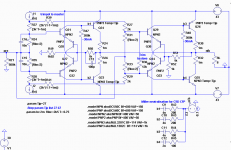
Update: A new idea is to use diodes Q5,Q6 (Post 1) as active devices. Then use them for the non-inverting input.
See attached (adapted from One of the Top Solid-State CFA amp design Post 539 sim4b).

My original circuit had symmetrical input resistances which is a distinguishing feature of VFA's.
This Rush input stage provides one high input resistance non-inverting input and a medium input resistance inverting input. This input asymmetry is a characteristic of CFA's. But now with a medium input resistance for the inverting input we can use higher value feedback resistors like those of a VFA. It can also be configured as a 4R differential amp; as shown Rin's to common are 11k non-inverting and 1k inverting.
The attached circuit shows a good gain and phase margin can still be obtained with the extra active transistors in the input stage by using a 2pF capacitor across the 15k feedback resistor. Dadod's VAS emitter bypass idea helps the PM a bit as well.
Any comments, suggestions are more than welcome. Feel free to use the idea. CFA opamp maker's might like to use it as well.
Cheers, Ian Hegglun
Update: A new idea is to use diodes Q5,Q6 (Post 1) as active devices. Then use them for the non-inverting input.
See attached (adapted from One of the Top Solid-State CFA amp design Post 539 sim4b).
My original circuit had symmetrical input resistances which is a distinguishing feature of VFA's.
This Rush input stage provides one high input resistance non-inverting input and a medium input resistance inverting input. This input asymmetry is a characteristic of CFA's. But now with a medium input resistance for the inverting input we can use higher value feedback resistors like those of a VFA. It can also be configured as a 4R differential amp; as shown Rin's to common are 11k non-inverting and 1k inverting.
The attached circuit shows a good gain and phase margin can still be obtained with the extra active transistors in the input stage by using a 2pF capacitor across the 15k feedback resistor. Dadod's VAS emitter bypass idea helps the PM a bit as well.
Any comments, suggestions are more than welcome. Feel free to use the idea. CFA opamp maker's might like to use it as well.
Cheers, Ian Hegglun
Attachments
I see a bouncing misconception here:
1- CFA omits one gain stage for feedback signal, for applications where a low impedance IN- signal is available. Balanced input by definition requires matched inputs, impedance and gain. (A buffer to fix that is not part of the CFA.)
2- Some of the schematics shown use no negative feedback loop. This is not CFA.
3- The usage of more B-E junctions in series with input signal increases distortion! The input impedance of bipolars is log(Ic).
4- "DC stabilization" (by usage of matched B-E junctions) looks a lot like "error cancellation" (by nulling the log(Ic) function with 1-log(Ic) in another transistor), but it is obviously not the same.
Buffer with gain using a Rush input stage
Hi Eva. Thanks for your thoughts.
I'm not sure you have noticed the novel part of my latest input stage in Post 3.
The Beta from Q8,Q9 has been added to the standard CFA inverting input.
The Beta's of Q6*Q13 and Q5*Q12 (two Beta's multiplied together) give a higher input resistance for the non-inverting input -- so it still has the same CFA property of asymmetrical input resistances.
Also the input resistance of the inverting input is still a reflection of the resistances seen by Q12,Q13 emitters but scaled by Beta's of Q8,Q9. These Beta's effectively give a transformer action, a two-way interaction -- so this new CFA configuration should still behave like a standard CFA -- except the input resistances are now scaled up.
The extra transistors Q8,Q9 will obviously add some extra phase shift. It trades some GBW for higher input resistance. Adding a small capacitor across the feedback resistor can overcome some of this. (With faster transistors the parasitic capacitance of the feedback resistor may be enough).
BTW I asked the question about whether this input stage can still be classified as a CFA in Post 647 here Current Feedback Amplifiers, not only a semantic problem?
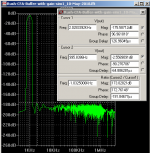
To give a better example of using this new input stage I have added a CFP follower. See attached circuit. It is intended as a buffer for adding to a power amplifier to give balanced inputs. It can drive 10Vpk into 1k ohms but normally 2Vpk for full output power. At 1V peak into 1k the THD is around 3ppb (-170dB) at 1kHz (see attached FFT plot).
In this example the output offset voltage is quite low at 0.3mV due to Rush pair's averaging out the PNP/NPN Vbe differences. Rush pairs trade some gain (~3 to 6dB) for a significantly lower offset voltage.
Hi Eva. Thanks for your thoughts.
I'm not sure you have noticed the novel part of my latest input stage in Post 3.
The Beta from Q8,Q9 has been added to the standard CFA inverting input.
The Beta's of Q6*Q13 and Q5*Q12 (two Beta's multiplied together) give a higher input resistance for the non-inverting input -- so it still has the same CFA property of asymmetrical input resistances.
Also the input resistance of the inverting input is still a reflection of the resistances seen by Q12,Q13 emitters but scaled by Beta's of Q8,Q9. These Beta's effectively give a transformer action, a two-way interaction -- so this new CFA configuration should still behave like a standard CFA -- except the input resistances are now scaled up.
The extra transistors Q8,Q9 will obviously add some extra phase shift. It trades some GBW for higher input resistance. Adding a small capacitor across the feedback resistor can overcome some of this. (With faster transistors the parasitic capacitance of the feedback resistor may be enough).
BTW I asked the question about whether this input stage can still be classified as a CFA in Post 647 here Current Feedback Amplifiers, not only a semantic problem?
To give a better example of using this new input stage I have added a CFP follower. See attached circuit. It is intended as a buffer for adding to a power amplifier to give balanced inputs. It can drive 10Vpk into 1k ohms but normally 2Vpk for full output power. At 1V peak into 1k the THD is around 3ppb (-170dB) at 1kHz (see attached FFT plot).
In this example the output offset voltage is quite low at 0.3mV due to Rush pair's averaging out the PNP/NPN Vbe differences. Rush pairs trade some gain (~3 to 6dB) for a significantly lower offset voltage.
Attachments
Thank you for taking the time...
...
to make the Rush pair more widely appreciated. Please accept my compliments on your kindness and patience and my congratulations on your excellent efforts to date.
My own fascination with this simple configuration spans a period of some considerable duration. Although now in retirement; almost rivalling the time spent many decades ago designing ECL in Silicon, which may be seen elsewhere to consist largely of LTP circuits.
As I am presently inclined towards avoiding these for audio applications, it is gratifying to see one of the forum's more well known contributors showing such a substantial interest in a Rush configuration.
There are, of course, a variety of means, with varying degress of symmetry, to bias the active pair(s). Architecturally; these may, perhaps in part, be characterised by their useage of current sources and the respective operating points emerging from such. Within this context, each choice impacts not only the measurable performance but also both the practical build and prospective survival of the final circuit.
Regarding the latter, key areas of concern being, as ever, the consequential clipping currents and particularly Base Emitter junction reverse potentials. In comparison with the ubiquitous LTP, these may be much more significant with Rush pairings. Equally so for spurious oscillations, even to the point of becoming hazardous to some transistor's continuing operation or impairing their longevity.
With respect to the buffer circuit you have posted; the attached .asc includes a small output capacitance to cover strays from interconnect and next stage input loading. The Tian probe results are shown in the following image and naturally, it will not run without oscillation.
In abstraction, to suggest that there is any concrete association between a given circuit topology and a properly viable compensation scheme is, at the very least, questionable. But once a configuration becomes fixed and critical locations acquire firm values from which the main performance benefits are derived. Then perhaps, less so. As is clear from Damir's impressive works. One without the other wants for a sensible completion.
In my brief examination of both the buffer and differential input circuits as recently posted here and in the other thread. The following observations; entirely from memory and without being in any way specific to a particular variant, may be of some small merit.
1) ULGF has a tendency towards being, for DIY, perhaps somewhat impractically excessive.
2) Generally, audio band gain is possibly unachievably high.
3) These prospective levels of performance may act to mask, in some areas, a circuit's substantive non linearites which would otherwise recieve a designer's attention.
4) From only a casual rooting around in some versions. Potentially destructive clipping currents and voltages may exist.
5) In some versions input stage currents are comfortably large enough to accomodate 'batch matched' vbe differences. In others this may not apply to quite the same extent.
6) From design to design in simulation; components useful to or even essential for stability seem to be included or not as they do or don't affect 'headline' performance parameters.
Thank you Ian.
This basic architectural approach is very interesting indeed.
It seems to me that it has good scope for further improvements. Not only for 'real world' performance and stability but also with respect to removing any tendencies towards component damage.
Cheers, ian
...
...
to make the Rush pair more widely appreciated. Please accept my compliments on your kindness and patience and my congratulations on your excellent efforts to date.
My own fascination with this simple configuration spans a period of some considerable duration. Although now in retirement; almost rivalling the time spent many decades ago designing ECL in Silicon, which may be seen elsewhere to consist largely of LTP circuits.
As I am presently inclined towards avoiding these for audio applications, it is gratifying to see one of the forum's more well known contributors showing such a substantial interest in a Rush configuration.
There are, of course, a variety of means, with varying degress of symmetry, to bias the active pair(s). Architecturally; these may, perhaps in part, be characterised by their useage of current sources and the respective operating points emerging from such. Within this context, each choice impacts not only the measurable performance but also both the practical build and prospective survival of the final circuit.
Regarding the latter, key areas of concern being, as ever, the consequential clipping currents and particularly Base Emitter junction reverse potentials. In comparison with the ubiquitous LTP, these may be much more significant with Rush pairings. Equally so for spurious oscillations, even to the point of becoming hazardous to some transistor's continuing operation or impairing their longevity.
With respect to the buffer circuit you have posted; the attached .asc includes a small output capacitance to cover strays from interconnect and next stage input loading. The Tian probe results are shown in the following image and naturally, it will not run without oscillation.
In abstraction, to suggest that there is any concrete association between a given circuit topology and a properly viable compensation scheme is, at the very least, questionable. But once a configuration becomes fixed and critical locations acquire firm values from which the main performance benefits are derived. Then perhaps, less so. As is clear from Damir's impressive works. One without the other wants for a sensible completion.
In my brief examination of both the buffer and differential input circuits as recently posted here and in the other thread. The following observations; entirely from memory and without being in any way specific to a particular variant, may be of some small merit.
1) ULGF has a tendency towards being, for DIY, perhaps somewhat impractically excessive.
2) Generally, audio band gain is possibly unachievably high.
3) These prospective levels of performance may act to mask, in some areas, a circuit's substantive non linearites which would otherwise recieve a designer's attention.
4) From only a casual rooting around in some versions. Potentially destructive clipping currents and voltages may exist.
5) In some versions input stage currents are comfortably large enough to accomodate 'batch matched' vbe differences. In others this may not apply to quite the same extent.
6) From design to design in simulation; components useful to or even essential for stability seem to be included or not as they do or don't affect 'headline' performance parameters.
Thank you Ian.
This basic architectural approach is very interesting indeed.
It seems to me that it has good scope for further improvements. Not only for 'real world' performance and stability but also with respect to removing any tendencies towards component damage.
Cheers, ian
...
Attachments
Thanks Ian (logician) for an affirmative post and for adding the Tian probe....
With respect to the buffer circuit you have posted; the attached .asc includes a small output capacitance to cover strays from interconnect and next stage input loading. The Tian probe results are shown in the following image and naturally, it will not run without oscillation.
...
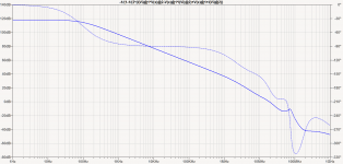
In my haste I didn't pay enough attention to getting a practical PM and didn't use the Tian probe before posting it. When I did use the Tian it was so close to oscillation, so you are right, any load capacitance will set it into oscillation.
Trying a few different values (C4,C5 500p and R16,R19 removed and C6 12p) I got at best a 3dB GM and 8 deg PM without chaning the Miller capacitors -- but still not enough with a 56pF load giving only a 5 deg PM.
Increasing the Miller capacitors will give a practical PM but the feedback factor at 1kHz has to reduce -- unless some other more effective compensation method is used that doesn't reduce the feedback factor as much. I'll leave that to other's who would like to refine the circuit.
It was intended as a buffer for giving balanced input resistances for CFA and VFA power amps but I may not need it right now.
@ padamiecki "depth of gnfb"?
The feedback factor at 1kHz is 97dB. So open loop THD would be ~0.03% at 1V. BTW The output stage is Class-A and when running at 1V output with about 20V max the open loop THD at 1V is around 0.03%.
@All
I have a stack of too many good ideas right now, so anyone who wants to use this is more than welcome to take it and use it.
It might be useful for headphone amps with some changes. I see a lot of interest in headphone amps and this one is fully discrete with no expensive bits like power amps.
Since this buffer can have voltage gain it could be used as a high output voltage swing 'preamp driver' for driving follower power stages, with suitable VAS cascode transistor voltage ratings you could get to 50V peaks.
Cheers, Ian Hegglun
Improved PM for Posts 5 & 8
Hi All,
A few more changes to compensation values to get a better PM without altering the Miller capacitor (so same THD):
increase input capacitor (C7) to 18-22pF, add R26,R27 100 ohms in series with Miller capacitors, change R16,R19 to 33 ohms, then add R28 100 ohms in output line.
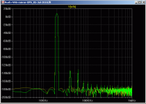
This gives GM 8dB PM 33deg with CL 56pF. The 100kHz 100ns rise time squarewave below with 56pF load. Circuits attached.

Increasing C7 input capacitor apparently does improve the PM by about 10 degrees, as well as attenuating the squarewave's higher harmonics so less ringing is seen.
Adding the 100 ohms resistors in series with the Miller capacitors add's about 10 degrees to the PM.
Adding the 100 ohm in the output line gives about the same PM with 56pF as no capacitor.
All this is a fairly academic exercise since the real THD difference of a real amp like this will be rather hard to measure at 1kHz when changing from 39pF to say 68pF Miller capacitors. Surely the noise floor will be higher than the THD (unless it is operated in liquid nitrogen), and then RFI ingress will be the killer (unless you can get 100km from any radio TV mobile phone towers).
But it is nice to know what tricks can squeeze a bit more PM out of a Miller compensated amp like this.
Hi All,
A few more changes to compensation values to get a better PM without altering the Miller capacitor (so same THD):
increase input capacitor (C7) to 18-22pF, add R26,R27 100 ohms in series with Miller capacitors, change R16,R19 to 33 ohms, then add R28 100 ohms in output line.
This gives GM 8dB PM 33deg with CL 56pF. The 100kHz 100ns rise time squarewave below with 56pF load. Circuits attached.
Increasing C7 input capacitor apparently does improve the PM by about 10 degrees, as well as attenuating the squarewave's higher harmonics so less ringing is seen.
Adding the 100 ohms resistors in series with the Miller capacitors add's about 10 degrees to the PM.
Adding the 100 ohm in the output line gives about the same PM with 56pF as no capacitor.
All this is a fairly academic exercise since the real THD difference of a real amp like this will be rather hard to measure at 1kHz when changing from 39pF to say 68pF Miller capacitors. Surely the noise floor will be higher than the THD (unless it is operated in liquid nitrogen), and then RFI ingress will be the killer (unless you can get 100km from any radio TV mobile phone towers).
But it is nice to know what tricks can squeeze a bit more PM out of a Miller compensated amp like this.
Attachments
CFA or not CFA? Question answered
I notice CPaul say's the same recently here Post 654 Current Feedback Amplifiers, not only a semantic problem?
Cheers
Thanks again Eva,I see a bouncing misconception here:
1- CFA omits one gain stage for feedback signal, for applications where a low impedance IN- signal is available. Balanced input by definition requires matched inputs, impedance and gain. (A buffer to fix that is not part of the CFA.)...
I notice CPaul say's the same recently here Post 654 Current Feedback Amplifiers, not only a semantic problem?
So my Rush input stage with a buffered inverting input (Posts 1 and 3) from the above precludes my versions from being a "CFA". My question answered.Whether employed in open or closed loop configurations, negligible portions of a VFA's input stage signal current come from its output or from a signal source external to the amplifier. But such current in a CFA comes only from such sources.
Cheers
Rush pairs for Class-AB+C
I have put 6 new amplifier designs on my website 'Showcase' directory (see my Sign links). My Class-AB+C amp is in the folder 'Foxtrot'. As I develop them further I will add more my website. Feel free to take any of my ideas and use them.
Class-AB+C is not new. It was discussed by John Broskie in TubeCad blog 177 here.
Class-AB+C uses a high-bias Class-AB stage with a second shunt Class-C stage. The Class-C stage is underbiased so that it starts to conduct when one of the Class-AB pair stops conducting. This keeps the gain constant rather than halving at high currents.
Effectively the crossover region is displaced from the centre region to higher power; with 500mA idle current crossover distortion is moved to several watts. Normal listening with music the crossover distortion happens much less frequently than standard Class-AB making it effectively disappear without needing to use gobs of negative feedback like standard Class-AB.
I have combined a Rush input stage (Post 3) with a Class-AB+C stage (see attachments) to see what it might achieve. It appears to be capable of solving most of the longstanding problems with Class-AB audio power amps.
The Class-AB+C stages use Current Source Driven (CSD) power transistors. This virtually eliminates thermal biasing problems. To speed up turn off I use Miller Neutralization by applying inverted collector voltage to the bases through a neutralization capacitor (like 1970's trannie radios used on their intermediate frequency stages).
Rush pairs are used for the driver transistors in the output stage. This allows a gain of 2 for the output stage without power feedback resistors. With a gain of 2 the VAS can operate from a lower voltage than the power rails. This simplifies power supplies.
I use TPOIC (Two Pole Output Inclusive Compensation) like Dadod 200W amp eg Post 1073 here. With TPOIC compensation I got about 20dB more feedback at 20kHz than Lag-lead and/or Miller Compensation.
Simulated distortion is 0.0004% (4ppm) at 100W and 20kHz with 500mA bias.
At 1W and 20kHz distortion falls to 0.1ppm (-140dB).
The attached plot show the distortion with the power transistors when Tj is stepped 27C and 67C.
There's no visible change when the power transistors heat up!
The input stage uses Rush pairs as in previous Post 3. With Rush pairs it can have balanced inputs using the 4R diff amp method. But as mentioned in Post 11 (above) it can't be called a CFA input stage because of the buffering of the feedback.
The present circuit is only for proof-of-concept for anyone is interested in these new idea. I haven't used suitable driver transistors for SOA for a 100W amp, nor output transistor SOA for 100W, nor bias compensation for the drivers. Miller neutralization requires a voltage inverter.
Cheers
....I have a stack of too many good ideas right now, so anyone who wants to use this is more than welcome to take it and use it...
I have put 6 new amplifier designs on my website 'Showcase' directory (see my Sign links). My Class-AB+C amp is in the folder 'Foxtrot'. As I develop them further I will add more my website. Feel free to take any of my ideas and use them.
Class-AB+C is not new. It was discussed by John Broskie in TubeCad blog 177 here.
Class-AB+C uses a high-bias Class-AB stage with a second shunt Class-C stage. The Class-C stage is underbiased so that it starts to conduct when one of the Class-AB pair stops conducting. This keeps the gain constant rather than halving at high currents.
Effectively the crossover region is displaced from the centre region to higher power; with 500mA idle current crossover distortion is moved to several watts. Normal listening with music the crossover distortion happens much less frequently than standard Class-AB making it effectively disappear without needing to use gobs of negative feedback like standard Class-AB.
I have combined a Rush input stage (Post 3) with a Class-AB+C stage (see attachments) to see what it might achieve. It appears to be capable of solving most of the longstanding problems with Class-AB audio power amps.
The Class-AB+C stages use Current Source Driven (CSD) power transistors. This virtually eliminates thermal biasing problems. To speed up turn off I use Miller Neutralization by applying inverted collector voltage to the bases through a neutralization capacitor (like 1970's trannie radios used on their intermediate frequency stages).
Rush pairs are used for the driver transistors in the output stage. This allows a gain of 2 for the output stage without power feedback resistors. With a gain of 2 the VAS can operate from a lower voltage than the power rails. This simplifies power supplies.
I use TPOIC (Two Pole Output Inclusive Compensation) like Dadod 200W amp eg Post 1073 here. With TPOIC compensation I got about 20dB more feedback at 20kHz than Lag-lead and/or Miller Compensation.
Simulated distortion is 0.0004% (4ppm) at 100W and 20kHz with 500mA bias.
At 1W and 20kHz distortion falls to 0.1ppm (-140dB).
The attached plot show the distortion with the power transistors when Tj is stepped 27C and 67C.
There's no visible change when the power transistors heat up!
The input stage uses Rush pairs as in previous Post 3. With Rush pairs it can have balanced inputs using the 4R diff amp method. But as mentioned in Post 11 (above) it can't be called a CFA input stage because of the buffering of the feedback.
The present circuit is only for proof-of-concept for anyone is interested in these new idea. I haven't used suitable driver transistors for SOA for a 100W amp, nor output transistor SOA for 100W, nor bias compensation for the drivers. Miller neutralization requires a voltage inverter.
Cheers
Attachments
Last edited:
Pretty cool, the core concept features the same number of transistors as the ADA4700-1 does (also a crossed 'rush' arrangement), although I suspect you enjoy better behaved input currents than the ADA without its input buffers. The ADA's execution only requires one side to have current sourcing to boot the entire circuit though.
I'm pretty pleased with how well my discrete variations of it work.
I'm pretty pleased with how well my discrete variations of it work.
I have put 6 new amplifier designs on my website 'Showcase' directory (see my Sign links). My Class-AB+C amp is in the folder 'Foxtrot'. As I develop them further I will add more my website. Feel free to take any of my ideas and use them.
Class-AB+C is not new. It was discussed by John Broskie in TubeCad blog 177 here.
Class-AB+C uses a high-bias Class-AB stage with a second shunt Class-C stage. The Class-C stage is underbiased so that it starts to conduct when one of the Class-AB pair stops conducting. This keeps the gain constant rather than halving at high currents.
Effectively the crossover region is displaced from the centre region to higher power; with 500mA idle current crossover distortion is moved to several watts. Normal listening with music the crossover distortion happens much less frequently than standard Class-AB making it effectively disappear without needing to use gobs of negative feedback like standard Class-AB.
I have combined a Rush input stage (Post 3) with a Class-AB+C stage (see attachments) to see what it might achieve. It appears to be capable of solving most of the longstanding problems with Class-AB audio power amps.
The Class-AB+C stages use Current Source Driven (CSD) power transistors. This virtually eliminates thermal biasing problems. To speed up turn off I use Miller Neutralization by applying inverted collector voltage to the bases through a neutralization capacitor (like 1970's trannie radios used on their intermediate frequency stages).
Rush pairs are used for the driver transistors in the output stage. This allows a gain of 2 for the output stage without power feedback resistors. With a gain of 2 the VAS can operate from a lower voltage than the power rails. This simplifies power supplies.
I use TPOIC (Two Pole Output Inclusive Compensation) like Dadod 200W amp eg Post 1073 here. With TPOIC compensation I got about 20dB more feedback at 20kHz than Lag-lead and/or Miller Compensation.
Simulated distortion is 0.0004% (4ppm) at 100W and 20kHz with 500mA bias.
At 1W and 20kHz distortion falls to 0.1ppm (-140dB).
The attached plot show the distortion with the power transistors when Tj is stepped 27C and 67C.
There's no visible change when the power transistors heat up!
The input stage uses Rush pairs as in previous Post 3. With Rush pairs it can have balanced inputs using the 4R diff amp method. But as mentioned in Post 11 (above) it can't be called a CFA input stage because of the buffering of the feedback.
The present circuit is only for proof-of-concept for anyone is interested in these new idea. I haven't used suitable driver transistors for SOA for a 100W amp, nor output transistor SOA for 100W, nor bias compensation for the drivers. Miller neutralization requires a voltage inverter.
Cheers
Excellent result. I called this compensation OITPC OITPC - Output inclusive TPC (not TMC) but TPOIC is equally good.
Damir
Oops
Oh I TP See. That's how I can remember it.")
I tried to look up what you called it but it got lost.
Does Bob Cordell or Douglas Self have a name for it or is it one of your creations?
Did you get to try the Rush idea in any of your amps?
Thanks for the like.
Hi Damir,Excellent result. I called this compensation OITPC OITPC - Output inclusive TPC (not TMC) but TPOIC is equally good.
Damir
Oh I TP See. That's how I can remember it.
I tried to look up what you called it but it got lost.
Does Bob Cordell or Douglas Self have a name for it or is it one of your creations?
Did you get to try the Rush idea in any of your amps?
Thanks for the like.
Did something similar My New CFB Frontend with balanced input biasing current requirements
Hi Damir,
Oh I TP See. That's how I can remember it.
I tried to look up what you called it but it got lost.
Does Bob Cordell or Douglas Self have a name for it or is it one of your creations?
Did you get to try the Rush idea in any of your amps?
Thanks for the like.
Hi Ian,
Not in their books, and I don't know anybody used it before.
No to much time for audio during summer, work around house and garden, start again in autumn and with the rush.
And I forgot about kASD circuit.
Damir
...Simulated distortion is 0.0004% (4ppm) at 100W and 20kHz with 500mA bias...
Hi Ian
That looks like fun, perhaps a bit optimistic with output transistors perfectly matched for BF and, less plausibly, for VAF.
I am curious about the stability, the Tian probe placement in the thumbnail may not be fully informative.
What does the Return Ratio look like?
Best wishes
David
Last edited:
That's cool. Back 2011 too!Did something similar My New CFB Frontend with balanced input biasing current requirements
The same as what I have apart from the 1k resistors for the noninverting part has trans-diodes for lower input offset voltage.
Thanks.
- Status
- This old topic is closed. If you want to reopen this topic, contact a moderator using the "Report Post" button.
- Home
- Amplifiers
- Solid State
- Has anyone seen Rush pairs used this way? For a CFA with true differential inputs