Decided to get brave and have a go at SMD power amplifier.
Had a few components going flying but got there in the end.
It didn't work first time as I had missed soldering a transistor leg.
Thank goodness for my speaker protector kit !
Some of the joints are a bit blobby but it works.
Had a few components going flying but got there in the end.
It didn't work first time as I had missed soldering a transistor leg.
Thank goodness for my speaker protector kit !
Some of the joints are a bit blobby but it works.
An externally hosted image should be here but it was not working when we last tested it.
Lead free solder is the bane of reliability costing $B in telecom spacecraft failures. Tin over time grows whiskers which eventually touch other parts and short out. It’s a myth that lead free is more reliable. Pb added to tin improves solderability and prevents tin whiskers.
Danger to lead-free electronics: tin whiskers - Technology & science - Science | NBC News
Don’t believe it? Here is a list of confirmed failures from tin whiskers.
Whisker Failures
Nice design NigelWright. I like working with SMt parts. You can get 150w from a pair of IRFPx240?
Danger to lead-free electronics: tin whiskers - Technology & science - Science | NBC News
Don’t believe it? Here is a list of confirmed failures from tin whiskers.
Whisker Failures
Nice design NigelWright. I like working with SMt parts. You can get 150w from a pair of IRFPx240?
Last edited:
Nice design NigelWright. I like working with SMt parts. You can get 150w from a pair of IRFPx240?
Luckily most of my SMD parts are miles apart.
The exception is the transistor legs which are quite close.
Maybe the smaller capacitors 1206's.
As to 150WRMS, yes its a optimistic claim.
Probably into a resistor.
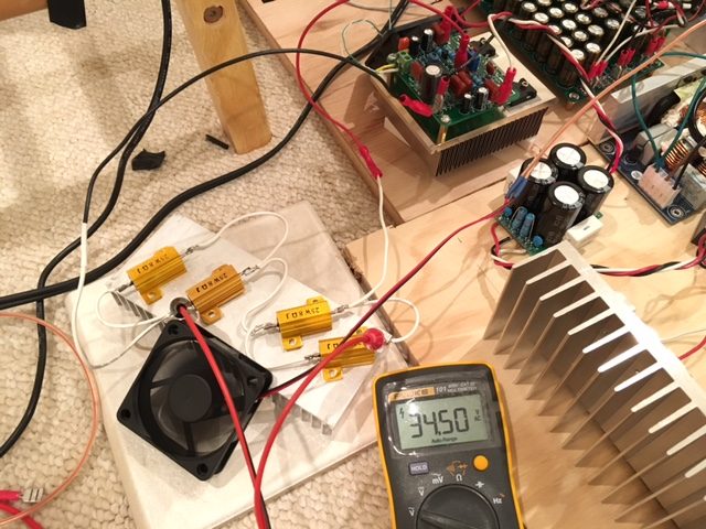
I actually managed 150w from a pair of IRFPx240’s with the FH9HV. I simply took a 50w design and boosted voltage rating on all transistors and caps. Then cranked it up and measured it. That was a big bank of 4 fancooled heatsinked 25w 8ohm resistors in series parallel. And they were hot! Got it to 34.5vrms into 8ohms. I think it can safely work at 125w for long duration though.
100W Ultimate Fidelity Amplifier
100W Ultimate Fidelity Amplifier
Last edited:
Did you design the PCB and are you going to let us see the schematic?
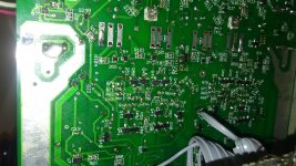
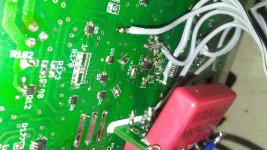
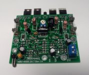
Yes I designed the pcb. I took standard SMD packages and extended pads a bit to make it easy to hand solder.
For through hole I usually use mpsa42/92 so used same transistors in SMD package.
An externally hosted image should be here but it was not working when we last tested it.
The circuit is based on a very old Hitachi lateral mosfet datasheet circuit
I changed to Vbe multiplier.
I added decoupling to front end as lateral mosfet version suffered from hum.
I also changed current mirror to two transistors instead of transistor and diode.
Here it is in pdf form:
150WRMS amplifier
I changed to Vbe multiplier.
I added decoupling to front end as lateral mosfet version suffered from hum.
I also changed current mirror to two transistors instead of transistor and diode.
Here it is in pdf form:
150WRMS amplifier
Last edited:
Don't forget to use lead free solder for the capacitors and resistors to avoid leaching of the tin with lead resulting in poor reliability.
Have you got a reference for this? I’ve used lead solder (SN63) exclusively both professionally and privately for ~30 years on many thousands of PCBs, using both lead/tin plated components and ROHS (tin plated) components.
The only reliability issues I’ve had is when ROHS BGAs have found their way into our process without being reballed with lead/tin balls. In this case the lead-free balls simply don’t reflow.
Luckily I work in an industry that’s ROHS exempt. I can’t begin to imagine the mess we’d be in reliability wise otherwise.
PCB looks great! Very neatly arranged layout. Plenty of space between parts, and I like the color") .....all I can get prototyped is standard green.
.....all I can get prototyped is standard green.  I use SMD quite a bit and have to say that the lead free stuff is much harder to use. It requires lots of heat and lots of flux but it can be used for larger SMD parts like you have there and maintain ROHS. I think you will like SMD, and find that you can go smaller, and pack more circuitry into smaller space. Next project you can shrink to 0805, Pd observed of course. ha. Now I typically use TINY SMD parts like 0402 size or SOT563. U7 in the first picture is SOT-23(8), a duel OP-AMP. I found that these buggers are not easy to hand solder.
 For multiple resistors packed in an array, I go with 0603 size, like 0603X2 or 0603X4 or 0603X8. This is about my limit, even with magnifier, my eyes not getting any younger. I actually tried 0201 size once but found it too difficult. Way too small.
  I used lead free solder once with this tiny stuff, it was a disaster. Very difficult to work with on such close spaces. With the leaded stuff, I don't seem to have as much problem with lifted pads. Very small pads are easy to lift with too much heat. I find that drawing the pad so that some of it if possible can be under the solder mask can help with lifted pad problems.
.....all I can get prototyped is standard green. I use SMD quite a bit and have to say that the lead free stuff is much harder to use. It requires lots of heat and lots of flux but it can be used for larger SMD parts like you have there and maintain ROHS. I think you will like SMD, and find that you can go smaller, and pack more circuitry into smaller space. Next project you can shrink to 0805, Pd observed of course. ha. Now I typically use TINY SMD parts like 0402 size or SOT563. U7 in the first picture is SOT-23(8), a duel OP-AMP. I found that these buggers are not easy to hand solder. For multiple resistors packed in an array, I go with 0603 size, like 0603X2 or 0603X4 or 0603X8. This is about my limit, even with magnifier, my eyes not getting any younger. I actually tried 0201 size once but found it too difficult. Way too small. I used lead free solder once with this tiny stuff, it was a disaster. Very difficult to work with on such close spaces. With the leaded stuff, I don't seem to have as much problem with lifted pads. Very small pads are easy to lift with too much heat. I find that drawing the pad so that some of it if possible can be under the solder mask can help with lifted pad problems.Attachments
Last edited:
I think one key to reliable SMT assemblies is to avoid using too much solder. Yes, once the solder melts the component tends to self-align on the pad due to surface tension effects of the liquid solder, ESPECIALLY with reflow processes. But if there's too much solder the component seems to drift randomly on top of the blob rather than aligning with the pad underneath it. And there's the problem of keeping the excess solder on top of the pads, not bridging over to adjacent pads.Some of the joints are a bit blobby but it works.
I have produced some SMT boards with a very uniform, smooth, appearance using solder paste and an electric skillet as a "Table-Top Reflow Oven". See Pad Holes Under SMT for Heat Sinking and other questions - Layout - KiCad.info Forums and Soldering paste for SMDs on HASL finished boards - Manufacturing - KiCad.info Forums . Like most things in life, your second attempt will have about 10% as many defects and shortcomings as the first time. And once the electric skillet has been used for soldering, whether leaded solder or not, it should never find its way back to anybody's kitchen.
I know it may be difficult to justify the cost for a one-off hobby project but applying solder paste with a stencil will save a significant amount of time compared to placing the solder paste with a syringe, reduce the re-work and cleanup time by at least half, and produce much more uniform results. See Stencil Manufacturing - Manufacturing - KiCad.info Forums . (Yes, I'm pleased with the products from OSH Stencils.) If your SMT footprints feature enlarged pads to make them more compatible with manual assembly techniques, the "paste shrink" parameter (reduction of stencil openings compared to pad size) should be more pronounced than what you use for automated SMT assembly methods.
Before you begin, cover your work table with plain white paper (such as white flip-chart paper, or paper tablecloth). Also consider covering the floor around your chair with white paper.Had a few components going flying but got there in the end.
For some reason, the SOT-23 packages give me the most problems in the reflow skillet method. If I place, say, half a dozen SOT-23 devices then I can count on one or more legs not getting properly soldered. Of course, the worst cases are when the joint is intermittent and makes or breaks as you handle the board. Some of those bad joints aren't obvious even under the desk magnifier - it takes a careful look with the toolmaker's microscope to even see the defect. I've taken to touching every SOT-23 pin with a soldering iron after reflow.It didn't work first time as I had missed soldering a transistor leg.
Dale
My worst problems come from uneven heating as function of time for hot skillet method - sometimes one pad melts first and surface tension will flip a chip resistor straight up like a fence post.
I found that solder paste can be applied and then each pad heated with a soldering iron tip even. It seems to provide a smoother fillet than using spool solder.
I found that solder paste can be applied and then each pad heated with a soldering iron tip even. It seems to provide a smoother fillet than using spool solder.
Can I just clarify the tin whiskers/solder situation. For us hobbyists (even in Europe) we do what we like as long as we are not caught. Facts are - 1) tin grows whiskers, 2) some other metals grow whiskers, but not as bad, 3) lead retards the growth of whiskers. The failures in satellites were not due to tin solder joints, because they're not used, they were due to bright tin plating. Something else worth considering is the use of gold-plating. When soldered there is migration and embrittlement. So remove gold from your component pads/leads/PCB with hot tin/lead before assembly. Courtesy of BAE Systems.
I have about half an inch (1.25cm) of common sand in the bottom of my skillet. Lightly pressing the board into the sand seems to even out the heating across the board.My worst problems come from uneven heating as function of time for hot skillet method . . .
I have a hot soldering iron handy when I'm doing boards in the skillet. At the end of the reflow time I touch any larger-than-most copper area, such as the collector tabs on power transistors or thermal pads under some IC's, as insurance that the solder has flowed well under the component where I can't see.
Dale
- Status
- This old topic is closed. If you want to reopen this topic, contact a moderator using the "Report Post" button.
- Home
- Amplifiers
- Solid State
- Latest project SMD 150WRMS power amplifier using vertical mosfets