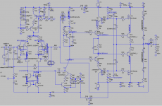
Did some revisiting of the "shared double bootstrap", which is convenient from a parts count and simplicity POV.
We can increase base/gate stoppers resistors. For example, in the following experiment I increased gate stopper R for the MOSFETs to 1K with no apparent harm. That will probably make the amp more stable...we can try different values there.
Other way to increase stability is by lowering gain, by increasing R4. In that experiment with R4=820r, gain is reduced to 16X but stability margins are better, before Zobel. For those who do not need a lot of gain or power. The same by reducing R feedback to 7K or so...10K is also nice.
I don't know if that will be detrimental for dynamics, though.
Also, I've been thinking about some for of isolation between bootstraps or from bootstraps to zeners, in the form of some low value resistor perhaps...
Attachments
Last edited:
Layout Considerations
Hi Max,
I'm using a semi-professional tool that combines schematic entry and layout
called Target 2001. Unfortunately this tool has no output for Gerber data.
but uses his own format. At least in Germany most of the PCB manufacturers
can work with this Target 2001 data without any problems.
Usually I need only 1 PCB, so I order a simple one layer PCB without solder mask due to the costs. Ordering let's say 5 PCBs is a different story.
PCB 100 x 140mm
2 layers with vias and 35um copper
solder mask on both layers, solder pads tin-plated (HAL lead free)
1 piece 55,00 Euro
2-5 pieces 76,70 Euro
15,45 Euro each
10 pieces 9,82 Euro
20 pieces 7,00 Euro
50 pieces 5,30 Euro
100 pieces 4,20 Euro
including value added tax and shipment within Germany.
I did not order any PCBs from this manufacturer so I have no experience
concerning quality. Since this is a professional manufacturer the quality should OK.
1 piece 55,00 Euro
2-5 pieces 76,70 Euro
15,45 Euro each
10 pieces 9,82 Euro
20 pieces 7,00 Euro
50 pieces 5,30 Euro
100 pieces 4,20 Euro
including value added tax and shipment within Germany.
Dear JOSI1,
I think 20 pieces at EU7 is cheap as can be. Lets go for it: I'll buy what it takes to go to that mark.

Two extra points:
Note that I no longer consider two separate emitter resistors (R21=200 Ohm) for the drivers, as my last schematics show. I will update the "TRIPLE".
I have to study the more complex compensation strategies as Symon recommended...
We need a bit more stability margins if others want to enter the project. There is a lot of responsibility there...
Though I am comfortable as it is for my own use.
Thanks again,
M.
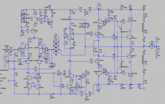
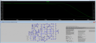
I already started the study of this very complex subject of compensation.
Please attached some of the trillions of variations possible.
I updated Symon's two-pole. Reduced C//R feedback to 15p. Note that I am using 4 resistors in // in my second amp, so that by itself adds some capacitance...
I added a simulation of a compensation with driver's stage included (I hope I remember well what the little bird told me...) which gives on paper good margins.
Also note that increasing current on the Drivers seems a good thing
The caps //zeners are not included because I did not like it in real world...
Opinions please.
Attachments
And the combination of the two techniques seems even more attractive.
Strangely enough, HF distortion does not appear...
Anyway, an easy mod to try...proabably will be a good radio emitter
Next I will include the whole output section...
Strangely enough, HF distortion does not appear...
Anyway, an easy mod to try...proabably will be a good radio emitter
Next I will include the whole output section...
Attachments
Hi Max,
I think the circuit in Post 226 defeats two pole compensation as the effect of C32 is shorted out by the output of the amplifier which is very low impedance. So C32 is mainly ensuring the junction of R21 and R48 is linked to the output.
I've not simulated this but I think it will show its working by single pole compensation. based on value of C10.
I'll post more when i get time
Regards,
Symon
That two-pole comp is very entertaining. A low cost, easy to test trick.
Of course, I will try every possible combination that seems stable on simulation.
If it appears stable, who am I to disagree?
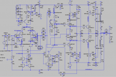
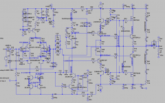
The thing is that I want to include drivers stage and/or output and see if that makes the CCS-loaded VAS amp stable. So far, it has been difficult to do so... after upgrading to boostrapped cascoded drivers.
For example the following gives best margins so far, as far (near) as I understand.
Oh! and I can also test what happens when current increases to 4.5mA on each tail of the input "pair".
Of course, I will try every possible combination that seems stable on simulation.
If it appears stable, who am I to disagree?
The thing is that I want to include drivers stage and/or output and see if that makes the CCS-loaded VAS amp stable. So far, it has been difficult to do so...
after upgrading to boostrapped cascoded drivers.For example the following gives best margins so far, as far (near) as I understand.
Oh! and I can also test what happens when current increases to 4.5mA on each tail of the input "pair".
Attachments
Hi Max,
i mentioned before that I'm concerned about connecting capacitors from Driver cascode Base to Ground, I know you found this kills oscillation in output. And at 1KHz it looks fine, but run the Dynamic simulation at 10KHz, and see what it does.
I'm playing with an alternative simplified cascode arrangement which I'll post later.
Also to evaluate stability it's useful need to simulate square wave behavior, as this shows up resonance problems.
Regards,
Symon
Hi Max,
i mentioned before that I'm concerned about connecting capacitors from Driver cascode Base to Ground, I know you found this kills oscillation in output. And at 1KHz it looks fine, but run the Dynamic simulation at 10KHz, and see what it does.
I'm playing with an alternative simplified cascode arrangement which I'll post later.
Also to evaluate stability it's useful need to simulate square wave behavior, as this shows up resonance problems.
Regards,
Symon
Ahem, if you teach me how to do it or if you post the .asc file, I will surely start doing it so...
For the strategy to deal with that oscillation, I copied the solution for one of the Ovation amps. I will try to run the cap directly to a star ground and see what this does.
Thanks, mate.
For the audience: we are dealing with the problems that arose after a complex output was chosen. I believe the amp will be stable if a common EF output version is built. In that way you still will be getting the effects of the LTMD.
In fact, you can, for example, take your own amp with Lin topology (or probably any amp with diff. pair input) an swap the input differential pair for a cascoded-CFP to get the taste of it...
Cheers,
M.
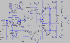
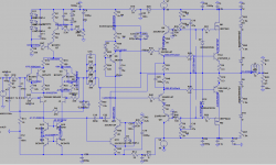
Hi Max,
I considered that the Driver stage cascode is basically doing the same as the OP device cascoe. so why duplicate?
Also since the OP cascode is a MOSFET it takes very little current, so we can reduce the boot strap current. Only problem is that the MOSFET cascode drop it too high for the driver so I had to increase the zener voltage.
I altered the feed back in the input stage so the input devices Q3 and Q5 now carry much less current than the complementary devices Q2 and Q4. I checked and in Peufeu's circuit he doesn't use emitter degeneration on the complemenrary devices so this shouldn't affect memory effect.
I test ran this at 1KHz, 10KHz, and 100Khz, and all seems stable in simulation.
What happens in real world?
Regards
Symon
Attachments
Hi Max,
I considered that the Driver stage cascode is basically doing the same as the OP device cascoe. so why duplicate?
Also since the OP cascode is a MOSFET it takes very little current, so we can reduce the boot strap current. Only problem is that the MOSFET cascode drop it too high for the driver so I had to increase the zener voltage.
I altered the feed back in the input stage so the input devices Q3 and Q5 now carry much less current than the complementary devices Q2 and Q4. I checked and in Peufeu's circuit he doesn't use emitter degeneration on the complemenrary devices so this shouldn't affect memory effect.
I test ran this at 1KHz, 10KHz, and 100Khz, and all seems stable in simulation.
What happens in real world?
Regards
Symon
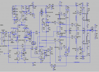
Brilliant. I will check it.
Playing with values and position of the CFP resistors is considered in the plan.
I know that the driver's cascode is the source of troubles so, appart your idea I will also test swapping transistors and even MOSFET cascode IF I can find medium power ones. Look at the attachment for my last exercise...but yours is a simplified version
so we are in tune...lets see what it does.Attachments
Hi Max,
I have some basic questions concerning:
C20
as far as I know this cap was recommended by D. Self to
improve the switching time of the output stage.
Did you detect any advantages (THD, stability) if this
cap is added.
Feedback from output signal
should one use separate traces from the output
to the feedback resistors (4x 50k) and
from output to C33 (bootstrap note)
Offset correction
Before introducing a double current mirror an offset correction
was possible by adding a trim pot to the 68R resistors.
How can an offset correction look like now.
Keep some small resistors (10R) in the emitter lines.
Using a resistor parallel to R13/R19=100
C19
C19=3300u/25V cap requires more board space for layout.
Can the capacity be reduced to 1000u or at least 2200u.
Double current mirror
should D13 and R47=100K be planned for layout
Hi Max,
I have some basic questions concerning:
C20
as far as I know this cap was recommended by D. Self to
improve the switching time of the output stage.
Did you detect any advantages (THD, stability) if this
cap is added.
I have always used this cap so I cannot comment. Maybe I'll experiment with different values.
Feedback from output signal
should one use separate traces from the output
to the feedback resistors (4x 50k) and
from output to C33 (bootstrap note)
The same trace works OK.
One good quality (low tempco) R would also be fine. From 10K (probably more stable) to 12.5K should work.
Offset correction
Before introducing a double current mirror an offset correction
was possible by adding a trim pot to the 68R resistors.
How can an offset correction look like now.
Keep some small resistors (10R) in the emitter lines.
Using a resistor parallel to R13/R19=100
I haven't implemented this mod yet. In fact I had to take a rest from the CCS-loaded VAS amp (made some upgrades to my digital projects instead) so no experiment this weekend. At the present time I cannot recommend that version because it seems more difficult to stabilize than the TRIPLE BOOTSTRAP amp.
I hope the cascoded curremt mirror will have perfect offfset...if not, we can try to degenerate a little, as you propose, one of the branches, depending of the signal value of the offset...
C19
C19=3300u/25V cap requires more board space for layout.
Can the capacity be reduced to 1000u or at least 2200u.
Again, I have not implemented this mod yet. Only the 100nF cap is there. The value does not seem that critical. Even a 47uF will do, so a 1000uF can be tried. I have here many Rubycon ZL 1800/35V caps with, I believe 12mm width.
Double current mirror
should D13 and R47=100K be planned for layout
They can be omitted..
Thanks for you patience.
Dear Symon,
I was thinking about your last proposal (not yet tried) but I am worried about Early voltage for the output BJT since now its VCE is much higher... in that case may be it would be better to let the drivers simple, meaning not cascoded.
I have tried both versions of the two pole compensation, with no effect on control of the oscillatory tendency of the CCS-loaded VAS amp, despite the wider margins they convey, so probably it is a local feedback problem...I have yet to try increased base resistors for the common-collectors and some BC caps...
Cheers,
M.
Hi Max,
you are correct, using the same MOSFet to cascode the output and driver does require a higher zerner voltage, but at least in simulation this doesn't seem to be a problem. The simulation file shows this, and a few other small changes to make it work.
i think for tis project the main advantage of cascode here is reduced power disipation in output and driver. So you get better bias stability, and less thermal memory effect.
But, the thing is try it and see how significant effect is of the output / driver cascode.
Regards,
Symon
Compensation is something that needs some further investigation, I'm playing with a 2 stage design currently, and while it appears stable I'm still looking for a better compensation solution before I start construction.
From previous practical experience you have to be careful adding capacitors to the circuit, sometimes they introduce new problems ... or just degrade performance to an un acceptable degree.
Yes, you are correct. After this project I promise to stick to 2 stage amps forever
My diffamp + single ended TOKIN VFET (2 stages of amplification) sounds great with my Autograph clones and I have almost all the parts to build another monster amp, with big heatsinks and all that...I even can do cascoded VFETs or depletion mosfet cascodying VFETs on the output.
I am also investigating how does the diffamp sounds when bootstrapped.
The goal is great dynamics and great transparency, but it seems hard to have both at the same time!
That is why I am attracted to cascodes and bootstraps...
Cheers,
M.
My diffamp + single ended TOKIN VFET (2 stages of amplification) sounds great with my Autograph clones and I have almost all the parts to build another monster amp, with big heatsinks and all that...I even can do cascoded VFETs or depletion mosfet cascodying VFETs
on the output.I am also investigating how does the diffamp sounds when bootstrapped.
The goal is great dynamics and great transparency, but it seems hard to have both at the same time!
That is why I am attracted to cascodes and bootstraps...
Cheers,
M.
Hi JOSI1,
About your thought:
I think I will give this topic a try: with smaller and bigger values and without. Thank you very much for the idea.
I was lazy because I put it underside the PCB...
M.
About your thought:
C20
as far as I know this cap was recommended by D. Self to
improve the switching time of the output stage.
Did you detect any advantages (THD, stability) if this
cap is added.
I think I will give this topic a try: with smaller and bigger values and without. Thank you very much for the idea.
I was lazy because I put it underside the PCB...
M.
Hi Max, JOSI1
As Max says the role of C20 is to speed up switch off of the "Slow" output devices, by giving the internal capacitor in the device a path to discharge. It works by allowing the driver for the device that is turning on to "Pull" the base of the output device that is turnng off and pulling out stored charge in the base capacitance. To do this C20 should be many times larger than the expected Cbe / Cob of the output devices. As with all things there is probably an optimal value.
So in general C20 makes the voltage drop between the base of output devices TTC2 and TTA2 more constant than just the resistor R21 + R48 would achieve. Incidently I think these resistor values are rather high, typically the value of the resistor in this position is lower. But perhaps C20 makes up for this?
Regards,
Symon
Yes, I simulated before lower values (50%) of these R21 R48 and it even helped THD a bit.
I don't no when I will have time to experiment though...
I think that could be one source of troubles.
When I increased the resistor from cascode's E to driver's C from 27 to 54 Ohm, the base oscillation dropped a bit on the mV range.
About that, I ordered a new scope probe since one of mine was old and suspect...
Thank you for your ideas.
M.
- Home
- Amplifiers
- Solid State
- The AMNESIS amp: a good amplifier, like a gentleman, has no memory.