Now let's go back to the inspiration.
Before anybody asks me: the only difference between models 5M20 and 5M21 was that the latter had VU-meters.
Most of the LTP parts were assembled separately on a discrete IC, which I won't be using on the Shadow. As you can see, no active part made it.
The parts inside the red lines will have to go on two piggy backs.
Attachments
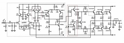
Another important thing I won't be able to keep on the Shadow is that the original amp was pure-DC, with no capacitor on the feedback.
Of course I will add a DC protection and I will try to see if that is possible on the Shadow. But I don't think it will. So the options are a feedback capacitor or a DC servo. I will try both ways and see which sounds better. Or at least more similar to the original Luxman.
Of course I will add a DC protection and I will try to see if that is possible on the Shadow. But I don't think it will. So the options are a feedback capacitor or a DC servo. I will try both ways and see which sounds better. Or at least more similar to the original Luxman.
Yes, the 5M20, B12, M12 and L10 are very similar, with usually minor details between each other. We will talk about them further on.
The M12 particularly is a very nice design, and it sims very very well. But neither I nor my friend, the one who owns the 5M21, have listened to it.
The M12 particularly is a very nice design, and it sims very very well. But neither I nor my friend, the one who owns the 5M21, have listened to it.
Perhaps what we are calling the pre-driver is just a buffer stage, like they used after the LTP. They used a similar configuration on the B12 and M12. But not on the L10.
The Luxman L10 is a very interesting amplifier, as it was a very well designed, high quality, mid-power integrated amplifier.
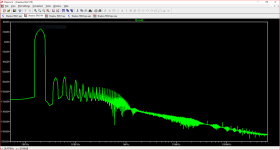
The L10 sims very very well, with very low THD at 1KHz and 20KHz. The only thing I could not tame, as I did in the 5M20, was a glitch in the sinusoidal in the LTP. The curve comes clean after the VAS. Someone told me that was on purpose, to increase linearity in later stages.
As usual I can upload the L10 asc simulations for anyone to see what I'm talking about, and comment about it.
Any minor departs from the original schematics, as I said about the changes I made, will be added gradually on the 5M20 prototype.
I suggest those interested on looking at Luxman's designs, to download the service manuals or schematics here:
Luxman | Hifi Manuals Free: Service Manuals, Owners Manuals, Schematics online for free download
The Luxman L10 is a very interesting amplifier, as it was a very well designed, high quality, mid-power integrated amplifier.
The L10 sims very very well, with very low THD at 1KHz and 20KHz. The only thing I could not tame, as I did in the 5M20, was a glitch in the sinusoidal in the LTP. The curve comes clean after the VAS. Someone told me that was on purpose, to increase linearity in later stages.
As usual I can upload the L10 asc simulations for anyone to see what I'm talking about, and comment about it.
Any minor departs from the original schematics, as I said about the changes I made, will be added gradually on the 5M20 prototype.
I suggest those interested on looking at Luxman's designs, to download the service manuals or schematics here:
Luxman | Hifi Manuals Free: Service Manuals, Owners Manuals, Schematics online for free download
Here go the sims I made with the L10.
If you ran the sine input signal, have a look at the spikes on the LTP. I wonder if it's something that can and/or should be corrected.
I tried several ways but I could not tame the spikes. But as I said, they disappear after the VAS stage.
The idling current per transistor pair is lower than on the 5M21. But increasing it practically does not affect THD. And the output bipolars double their heat.
C10/12 are zero on the original schematic.
Attachments
If you ran the sine input signal, have a look at the spikes on the LTP. I wonder if it's something that can and/or should be corrected.
It's the cascode that gives you trouble...try without one
")
I think not. For several reasons.
1) Eliminating the cascode would mean a big change in the original design, because a lot of things would have to be changed. That's not the idea of this project.
2) The other amps in this "family" do not have this problem, or can be corrected. Maybe the buffer they have after the VAS is the reason why.
3) Cascodes are a very good thing for linearity, even if Doug Self prefers mirrors to them.
Isn't there any other way to tame those spikes?
To eliminate the cascode I would have to lower the supply for the input stage, which I definitely will not do. So no need to simulate that. Too many changes to do.
But trying the DML-02 on LTP is easy. That I will try.
Some people told me the problem was in the feedback from the drivers. Doing that is how I tamed the spikes on the 5M21. But if those spikes were done on purpose, as it was also suggested, then I would be changing the designer's intentions. Even on the 5M21.
That's why my intention on the 5M21 was to add the simulated changes after listening to the prototype without them.
I have run simulations on the Shadow 5M21 version you have prototyped.
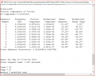
You mentioned fitting C306 and C307 both 270 pF to the back of the pcb - testing the THD with a 2uF parallel cap and 8R on 20 kHz sine wave there was no real difference with 0.89 volts input.
By the very finest of margins leaving them out was better under those conditions - but the situation could be reversed at a lower signal input and a lower frequency although I have not looked.
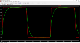
I also looked at the 10 kHz square wave test - the circuit holds up well with a 2uF parallel with 8 R showing the feedback loop is stable.
It remains that way with the supply voltages for the latter stages increased from 50 volts to 60 volts if that is in the plan for your final show piece version.
Congratulations on these fine results - I'm impressed here are some screen shots to bear witness.
You mentioned fitting C306 and C307 both 270 pF to the back of the pcb - testing the THD with a 2uF parallel cap and 8R on 20 kHz sine wave there was no real difference with 0.89 volts input.
By the very finest of margins leaving them out was better under those conditions - but the situation could be reversed at a lower signal input and a lower frequency although I have not looked.
I also looked at the 10 kHz square wave test - the circuit holds up well with a 2uF parallel with 8 R showing the feedback loop is stable.
It remains that way with the supply voltages for the latter stages increased from 50 volts to 60 volts if that is in the plan for your final show piece version.
Congratulations on these fine results - I'm impressed here are some screen shots to bear witness.
Attachments
Thanks, Mjona. The merit is Luxman's, as you certainly guess.
I'm very much curious on how and if those very good sims turn into an good sounding amp.
About the "correcting parts", hopefully I will be able to listen if something changes in the sound when every one is soldered in. The cap that I didn't put in the schematic was the capacitor between base and emitter that Keantoken had suggested to compensate for the additional capacitance in the original transistor.
That cap did change THD, as well as the frequency response and phase in the higher side of the curve.
If you can, join the mid of the drivers emitter resistors to the output, and look at the spikes on the LTP sinus signal.
Thanks, Mjona. The merit is Luxman's, as you certainly guess.
I'm very much curious on how and if those very good sims turn into an good sounding amp.
About the "correcting parts", hopefully I will be able to listen if something changes in the sound when every one is soldered in. The cap that I didn't put in the schematic was the capacitor between base and emitter that Keantoken had suggested to compensate for the additional capacitance in the original transistor.
That cap did change THD, as well as the frequency response and phase in the higher side of the curve.
If you can, join the mid of the drivers emitter resistors to the output, and look at the spikes on the LTP sinus signal.
Taking your last point first I tested this with a 20 k sine input to see the shape of the wave at node 004 which connects R205 to Q3 collector and there are notches at the peak and trough.
When the link is cut the notches are still there but are much lower in magnitude.
There are Miller capacitors providing local high frequency feedback around various transistors further down the amplification chain - see in the positive circuit half looking at Vn06 i.e. Q302 emitter, and , rather cutely in the negative circuit half one stage later at Vn036 i.e. Q305 emitter.
In that manner you can identify the points where the notches disappeared and see the progressive effects of Miller compensated stages.
There is an extremely fine margin in the THD simulation when the 270 pF capacitors are in circuit or not.
You are using higher performance output devices with 30 MHz unity gain capability against original types with 10 MHz and 15 MHz specification while the circuit still uses compensation capacitor values around the voltage gain stage appropriate to the older devices.
The simulation says your amplifier will deliver high power low distortion at 20 kHz into 8R//2uF - no small achievement.
270 pF capacitors may have been useful as insurance in the early development of this circuit but there has been one small but significant change where C207 - a 33pF Miller capacitor in the original circuit was increased to 150 pF.
In my view that change makes the 270 pF ones redundant.
Last edited:
- Status
- This old topic is closed. If you want to reopen this topic, contact a moderator using the "Report Post" button.
- Home
- Amplifiers
- Solid State
- When a Luxman clone is not a clone