Hi!
After building tube amplifiers for a while, and parallel to it, I want to design and build a simple SS audio amplifier. My target output power is just about 3W.
I'm about to build a JLH class A amplifier, and there're lots of good class A and AB designs out there. But in the pursuit of gaining understanding, I want to build something I can design and fully understand by myself. So, I'm seeking for some help.
Thus, I'm not looking for great performance, just decent sound quality, and on top of all, clarity.
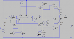
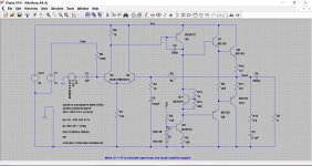
I attached my design, as image and LTspice circuit.
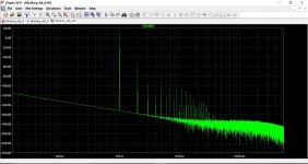
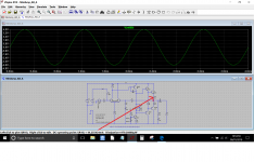
The simulations seem good enough.
Suggestions are very much appreciated!
After building tube amplifiers for a while, and parallel to it, I want to design and build a simple SS audio amplifier. My target output power is just about 3W.
I'm about to build a JLH class A amplifier, and there're lots of good class A and AB designs out there. But in the pursuit of gaining understanding, I want to build something I can design and fully understand by myself. So, I'm seeking for some help.
Thus, I'm not looking for great performance, just decent sound quality, and on top of all, clarity.
I attached my design, as image and LTspice circuit.
The simulations seem good enough.
Suggestions are very much appreciated!
Attachments
Well, there are a few points here. I don't know where the best place is to read up on the issues, but Self's and Cordell's books appear to be good places to start.
My "first thoughts" comments are:
(1) classical Miller compensation (your 200pF) and low input stage current (600uA per device in the input stage?) and 6k resistor do not seem to be optimum (the 6k needs 100uA, so the currents may be unbalanced) and likely to suffer "hard" slew induced distortion.
(2) I'm sure you don't really want 330 ohms feeding the bias diodes for the VAS load transistor which again is running low, (at around 1mA?), and too low to drive your compensation capacitor. More like 6k from 12v would supply 2mA which would be enough to bias the VAS transistor constant current load, which should probably run at 10mA. (Some would say 6mA but I've previously commented that I think that is too low too).
(3) Not sure whether BD139/BD140's can handle 1A with any gain. While some manufacturers rate these as 1.5A the gain spec. shows a fall-off at 500mA. I'd recommend using higher power output transistors. Several TO-220 types available.
(4) Current mirrors need balancing resistors (input stage tail current) as thermal coupling is not 100% and transistor mismatch can give rise to big variations unless carefully matched.
Last edited:
I agree you could build a single stage Class A 3W amplifier, perhaps using 3 transistors.
You could probably build a 5-transistor AB circuit for 3W that has low distortion too.
But I took the post to be looking for assistance in learning about a Class AB. For 3W into 8 ohms that's going to need almost 1A peak output. That is not difficult, but it is still not quite so simple, unless you specify high gain transistors. So I'd stick with the standard design, but with some changes. Though I have designed three transistor Class A 4W amplifiers using an output transformer too.
@elerion - is your objective to understand class AB or design a simple 3W amplifier?
Last edited:
I agree. If your goal is sound quality then use a class A, single ended output. 700mA to 1A bias.3 Watt;-? Little SE;-! 1 - 2 stages.
NO push-pull!
NEVER complementary-parts-pp;-!!!
Since you have chosen to capacitor couple the input and output (which I think is a good decision for a first project!), you have the opportunity to simplify the power supply and save some big heavy components. Rather than plus-and-minus 12V, how about +24V and ground. Only.
I agree with the earlier commenter who suggests emitter resistors for Q1 and Q2, to ameliorate the effects of not-perfectly-matched transistors. The standard advice is to choose resistor values which give about 500 millivolts of voltage drop across the emitter resistors. Since you're already using LTSPICE, the necessary experiments are quick and simple.
I also recommend that you use LTSPICE to study the DC collector currents of the input transistors Q3 and Q4. Douglas Self's book is correct: you want these currents to be equal: within 1% of each other would be ideal. You may need to adjust R1 and/or R8 to get the perfect balance you seek. Remember that this will affect the gain of the amplifier as a whole.
Last edited:
Self's and Cordell's books are great, but jumping into practice is sometimes difficult. So many things to consider.
Thanks john_ellis for your comments, I will definitely think about it and apply it the best I can.
I know it could be a class A. But I want to do an AB desing, that I can evolve latter. And, on top of everything, gain a deeper understanding.
My objective is thus to understand class AB. If it is low power, better. So I can use smaller transistors, and smaller heatsinks. This will be my first project using decent heatsinks. I think "step a time" is the best way to learn.
By the way, in the LTSpice circuit I included a class A version of the amplifier. Just the Vbe multiplier changes.
Last edited:
I think you are starting out with something that is contrary to what you stated your goals are: simple and sounds great. The JLH design is not simple. People treat it like it's simple. If you have tube design knowledge and you are new to solid state then I would really advise starting a lot simpler than this. You will learn more.
And avoid textbooks by authors who don't listen critically to their own theories.")
And avoid textbooks by authors who don't listen critically to their own theories.
I would also say that if you really want to understand how an AB amp works then you need to start with just the absolute basics such as a complementary pair of output transistors (and nothing else) and see for yourself how they behave in isolation... and then look at building on that to create a circuit.
What you show in post #1 is quite a full featured design needing only a little refinement.
Simulation makes all that easy and non destructive of course.
What you show in post #1 is quite a full featured design needing only a little refinement.
Simulation makes all that easy and non destructive of course.
Oh, the JLH project is not for learning, just for building and use. I more or less understand it, which is enough at this point.
Mooly, that design I posted is done the way you recommend me.
It took me a lot of time. I didn't copy it from any other source.
I read, read, read,.... theory. Then I spent hours simulating all the blocks isolated.
I started with the LTP though. I know it usually the other way round what is recommended.
It is what I do with tube amplifiers, because I understand better how power and gain is achieved.
I just waited to have something, before asking for help, as some people do.
This is why your help's got a great value for me.
Last edited:
I'd have to see a link to what I said I honestly don't just recall it.
Well your design in post #1 looks basically OK, however you should look at R5 as 330 ohm is way to low and will be forcing a lot of current into the diodes. Using single rail is a good idea as was mentioned. You might find making the gain considerably higher will help in both stability and subjective sound quality. The bias generator needs to be adjustable. Finally the LTP input stage needs the tail current sink looking at imo.
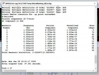
I'll have a closer look at your simulation later.
I honestly don't just recall it.Well your design in post #1 looks basically OK, however you should look at R5 as 330 ohm is way to low and will be forcing a lot of current into the diodes. Using single rail is a good idea as was mentioned. You might find making the gain considerably higher will help in both stability and subjective sound quality. The bias generator needs to be adjustable. Finally the LTP input stage needs the tail current sink looking at imo.
I'll have a closer look at your simulation later.
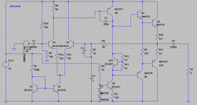
Following all of your advices:
- I added emitter resistors to LTP. (50 millivolts quiescent voltage drop)
- I balanced LTP currents, lowering the tail's CSS current.
- I raised VAS CSS current (>6mA) and lowered diode biasing.
Finally I thought on using to-220 tip31/tip32 instead bd135/bd136.
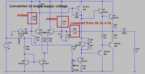
Now, I had some trouble making the single supply voltage modification.
I attached the related changes. I might have done something wrong.
Even though I suppose, I don't really fully understand why I had to half the feedback resistor from 9k to 4.5k.
- I added emitter resistors to LTP. (50 millivolts quiescent voltage drop)
- I balanced LTP currents, lowering the tail's CSS current.
- I raised VAS CSS current (>6mA) and lowered diode biasing.
Finally I thought on using to-220 tip31/tip32 instead bd135/bd136.
Now, I had some trouble making the single supply voltage modification.
I attached the related changes. I might have done something wrong.
Even though I suppose, I don't really fully understand why I had to half the feedback resistor from 9k to 4.5k.
Attachments
Have a look at this as a basis to work from. Points addressed...
1/ Input biasing is derived from a stable reference voltage rather than the main rail (which would allow injection of noise and hum into the amplifier input. The reference voltage can be a suitably decoupled zener, perhaps higher in voltage than needed, and with a preset to allow adjustment of the midpoint voltage.
The input impedance is now much higher as well.
2/ The LTP tail has just a simple resistor at this stage.
3/ The feedback return is AC coupled.
4/ The diodes are now fed with around 1.5ma
5/ The VAS current is increased to around 3.5ma via R2
6/ R13 is set to give around 40ma bias current.
7/ A Zobel network is added to the output to correctly terminate the amplifier by appearing as a load of reducing impedance relative to frequency. This greatly aids stability.
(You will need to add your own .lib models back)
Attachments
The 1k feedback return needs to be AC coupled.
That was it! Thank you.
I just placed a huge capacitor, to fix the value later.
Use this circuit instead of the one I originally posted.
24 V single supply, and all the recommendations you guys pointed out.
(I posted this before seeing Mooly's previous post)
Attachments
- Status
- This old topic is closed. If you want to reopen this topic, contact a moderator using the "Report Post" button.
- Home
- Amplifiers
- Solid State
- Help with design for a simple low power audio amplifier