I acquired a smashed, non working Sony TA-5650 VFET amp for peanuts on eBay earlier this year. It may have fallen down or some heavy object may have fallen over it.
Visual inspection revealed the sturdy chassis was bent on the floor (!) and the roof was deformed also. The volume control (“equalizer”) PCB was broken.
Apart that, I found only one resistor was burnt at the 70V power supply PCB. All VFETs were good and all VD-1221 diodes were also good.
After performing all the recommended upgrades that the net could bring, I discovered one channel was sounding good (very good) and the other collapsed the voltages, which is a constant complaint in several fora: I checked and it was oscillating as soon as I connected PRE (or any source) to AMP jacks.
The scope showed a 200KHz oscillation...quite low I suppose. During the next months I tried several tricks but none cured the ailment...what a disappointment. Such a nice amp…
Recently I found an article about a Leach amplifier from Georgia Tech that explained to me how the complementary common-source amplifier output is prone to oscillation and why the pre-drivers and drivers were all connected to feedback loop.
Apparently Miller capacitance of the power device still was able to produce oscillation even with all the measures the Sony engineers had taken to combat it.
Well, I do not fully understand this but it certainly has to do with time constants plus gain-bandwidth...I don't have the knowledge to manipulate those at will and my silly attempts prove fruitless, but I know some trick that will reduce Miller effect to negligible levels: cascoding the power devices, like I am doing in several of my amps, since I got acquainted with the Sony TA-N7B circuit, but this time, all the way around, with the BJT (2SA1173/2SJ473) in common-Gate. I took a deep breath and made the modification...and it worked. The channel is stable now and produces nice music. I haven't tried to force it yet, making power and frequency response tests...I am still worried and fearful, but with only one pair VFET per side I reached about 15Watts without problem, which is fine for me until now.
The added advantage of using those good sounding, low power old BJTs in cascode is that they should protect the VFETs and sacrifice themselves in case of high current, right?
I think, due to the good results (functional power amp) I will cascode the other channel and try the full cavalry of 8 VFETs, though by cascoding I loose around 5 Volts of headroom per side...what is that for an 8 Ohm load?
Some questions for The Wise:
By extending the power-bandwith through cascoding, will the amp be prone to oscillate at higher Fs?
I guess Sony engineers implemented the usual protective measures well.
Can I improve things, now that the amp is stable, like making the pre-drivers work in class A?
Can I implement a better bias control circuit?
An intriguing adverse effect of my mod (or was it a prior mistake?) is that the bias current control is no longer working! It runs steadily at very low bias, close to class B, I guess, but the VFETs do work, with VGS of 15V last time I checked.
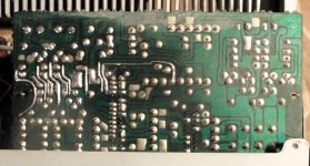
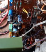
To isolate potential problems, I bypassed the “filter board” so volume control comes directly from “equalizer board”, to keep Sony's bulletin nomenclature. I updated JFETs, filter caps, coupling caps there and it sounds good to me. You will see in the picture I use everywhere I could Vishay MKT//Russian army surplus polystyrene caps. Very transparent combination IMHO.
I hope you leave your comments and recommendations.
Greetings,
M.
PS: I will show later a diagram of my cascode mod.
Visual inspection revealed the sturdy chassis was bent on the floor (!) and the roof was deformed also. The volume control (“equalizer”) PCB was broken.
Apart that, I found only one resistor was burnt at the 70V power supply PCB. All VFETs were good and all VD-1221 diodes were also good.
After performing all the recommended upgrades that the net could bring, I discovered one channel was sounding good (very good) and the other collapsed the voltages, which is a constant complaint in several fora: I checked and it was oscillating as soon as I connected PRE (or any source) to AMP jacks.
The scope showed a 200KHz oscillation...quite low I suppose. During the next months I tried several tricks but none cured the ailment...what a disappointment. Such a nice amp…
Recently I found an article about a Leach amplifier from Georgia Tech that explained to me how the complementary common-source amplifier output is prone to oscillation and why the pre-drivers and drivers were all connected to feedback loop.
Apparently Miller capacitance of the power device still was able to produce oscillation even with all the measures the Sony engineers had taken to combat it.
Well, I do not fully understand this but it certainly has to do with time constants plus gain-bandwidth...I don't have the knowledge to manipulate those at will and my silly attempts prove fruitless, but I know some trick that will reduce Miller effect to negligible levels: cascoding the power devices, like I am doing in several of my amps, since I got acquainted with the Sony TA-N7B circuit, but this time, all the way around, with the BJT (2SA1173/2SJ473) in common-Gate. I took a deep breath and made the modification...and it worked. The channel is stable now and produces nice music. I haven't tried to force it yet, making power and frequency response tests...I am still worried and fearful, but with only one pair VFET per side I reached about 15Watts without problem, which is fine for me until now.
The added advantage of using those good sounding, low power old BJTs in cascode is that they should protect the VFETs and sacrifice themselves in case of high current, right?
I think, due to the good results (functional power amp) I will cascode the other channel and try the full cavalry of 8 VFETs, though by cascoding I loose around 5 Volts of headroom per side...what is that for an 8 Ohm load?
Some questions for The Wise:
By extending the power-bandwith through cascoding, will the amp be prone to oscillate at higher Fs?
I guess Sony engineers implemented the usual protective measures well.
Can I improve things, now that the amp is stable, like making the pre-drivers work in class A?
Can I implement a better bias control circuit?
An intriguing adverse effect of my mod (or was it a prior mistake?) is that the bias current control is no longer working! It runs steadily at very low bias, close to class B, I guess, but the VFETs do work, with VGS of 15V last time I checked.
To isolate potential problems, I bypassed the “filter board” so volume control comes directly from “equalizer board”, to keep Sony's bulletin nomenclature. I updated JFETs, filter caps, coupling caps there and it sounds good to me. You will see in the picture I use everywhere I could Vishay MKT//Russian army surplus polystyrene caps. Very transparent combination IMHO.
I hope you leave your comments and recommendations.
Greetings,
M.
PS: I will show later a diagram of my cascode mod.
Attachments
Last edited:
I'm sorry to say you do not seem to understand how the N7 circuit works. As far as the previous stages are concerned, the output is a standard BJT output, so the drivers in the 5450 circuit are completely NOT suitable, the whole thing would have to be pulled out.
The original bias circuit provides negative bias and NO thermal compensation, which is exactly the opposite of what is required for BJTs.
This oscillation issue has been explored here before.
It has to do with two things:
1) signal ground is routed all around the amp and any contact problems between the input connector and local ground will drive the amp crazy as it's entire input stage loses ground (reference). There are two nearby points on the PCB where the input ground and power ground are oposed with about 2cm of space, a 4.7 ohm resistor in parallel with 100pF cap should be mounted there. Also, local decoupling of the main power rails (44V) is recommended.
2) The driver transistors degrade, and they are not complementary. Replacement with something like 2SB649/2SD669 will work (even MJE340/350 if you really must!) but the small capacitances in the driver stages must be slightly increased (C310,313) to around 18-22pF.
3) Series gate resistances for the VFETs are very small. To be honest I have no idea why, VFETs are very fast and have a low capacitance even accounting for Miller effect. Also, they are different on the P and N VFET side, by a factor of 2, which is even stranger since the input capacitance of the VFETs is quite nicely balanced. The driver stage can still be marginal for oscillation unless these are increased, to 33 ohms (instead of 10) and 47 ohms (instead of 22).
If you got this amp for a pittance, remember that a working set of VFETs will set you back around 400-450 US$ IF you can find genuine parts (in general, don't even think of it without being able to curve trace them as what is written on them and what you get will almost certainly be two different things). Not something to be played with lightly. This is really NOT an amp to experiment on unless you have a LOT of previous experience and if possible with VFETs.
Last edited:
Happy year 2018 to all the brave amplifier builders! 
Dear Ilimzn, thank you for your extensive and detailed reply. I am sad to think that my poor description induced you to a wrong conclusion.
I meant I was inspired by N7 to explore cascodying the output section of amplifiers, not that I copied the same. My amp is still the same 5650 VFET amp, safe that VFET's sources are not fed directly from +/- 44V power supply but from BJT's emiters (+/-39V) in common-gate. I should make a diagram as time allows...
Indeed, there are several decisions taken by Sony engineers that seem odd, as you comment. I believe they realized that the amp was marginally stable, so they went on with all these mods to pass the tests.
I only missed the ground-connect-through resistors mod, to be honest.
I do believe my ground is solid since the amp has been stable since the cascodying, but I'll try it ASAP. Signal and power ground are 1mm apart, so the decision to separate them probably was due to fear of introducing PS HF currents into the input, thus inducing oscillation. Added capacitance to power pins is wise and was done.
Anyway, I don't want my amp to be marginally stable but very table no matter what, so I tend to believe that my cascodying mod is good and even I suspect the amp will be better sounding than the original, as has been the case with my two other amps that I cascoded: the VSSA from Lazy Cat and the DX Blame ST from Destroyer X. They simply sound more like music to me.
Thanks again for your interest and help,
Cheers,
M.
Dear Ilimzn, thank you for your extensive and detailed reply. I am sad to think that my poor description induced you to a wrong conclusion.
I'm sorry to say you do not seem to understand how the N7 circuit works. As far as the previous stages are concerned, the output is a standard BJT output, so the drivers in the 5450 circuit are completely NOT suitable,
I meant I was inspired by N7 to explore cascodying the output section of amplifiers, not that I copied the same. My amp is still the same 5650 VFET amp, safe that VFET's sources are not fed directly from +/- 44V power supply but from BJT's emiters (+/-39V) in common-gate. I should make a diagram as time allows...
This oscillation has to do with two things:
1) signal ground is routed all around the amp and any contact problems between the input connector and local ground will drive the amp crazy as it's entire input stage loses ground (reference). There are two nearby points on the PCB where the input ground and power ground are opposed with about 2cm of space, a 4.7 ohm resistor in parallel with 100pF cap should be mounted there. Also, local decoupling of the main power rails (44V) is recommended.
2) The driver transistors degrade, and they are not complementary. Replacement with something like 2SB649/2SD669 will work (even MJE340/350 if you really must!) but the small capacitances in the driver stages must be slightly increased (C310,313) to around 18-22pF.
3) Series gate resistances for the VFETs are very small. To be honest I have no idea why, VFETs are very fast and have a low capacitance even accounting for Miller effect. Also, they are different on the P and N VFET side, by a factor of 2, which is even stranger since the input capacitance of the VFETs is quite nicely balanced. The driver stage can still be marginal for oscillation unless these are increased, to 33 ohms (instead of 10) and 47 ohms (instead of 22).
.
Indeed, there are several decisions taken by Sony engineers that seem odd, as you comment. I believe they realized that the amp was marginally stable, so they went on with all these mods to pass the tests.
I only missed the ground-connect-through resistors mod, to be honest.
I do believe my ground is solid since the amp has been stable since the cascodying, but I'll try it ASAP. Signal and power ground are 1mm apart, so the decision to separate them probably was due to fear of introducing PS HF currents into the input, thus inducing oscillation. Added capacitance to power pins is wise and was done.
Anyway, I don't want my amp to be marginally stable but very table no matter what, so I tend to believe that my cascodying mod is good and even I suspect the amp will be better sounding than the original, as has been the case with my two other amps that I cascoded: the VSSA from Lazy Cat and the DX Blame ST from Destroyer X. They simply sound more like music to me.
Thanks again for your interest and help,
Cheers,
M.
Last edited:
Well, cascoding is no magic and in particular cascoding the output is a whole different proposition. It's a circuit topology, not a magical cure. I do not remember VSSA or DX Blame ST having cascoded VFETs in the outputs? So I do't understand how this can even compare???
Again, converting the output to N7 style cascoding COMPLETELY changes the operation. At the very least you are now driving a current controlled device rather than a voltage controller one, with wildly different requirements - high current low voltage, instead of low current high voltage. Completely unsuitable for the original driver, hence no idle current. And if you had idle current, it's not temperature servoed so it WILL go into thermal runaway. So, now you have a 'stable' amp with no idle current = high distortion.
Let me make it clear again: if you connect a N VFET as the top of the cascode (gate grounded, or in this case connected to the +44V rail) and the bottom device is a BJT (base=input, emitter on +44, collector on VFET source), your composite device BEHAVES AS THE BJT, NOT THE VFET!!! And it requires bias below the +44V rail, not above (towards the +75V rail, like a VFET, AND it requires a fairly large amount of base current, not very litle current and high voltaga sweing like the VFET. Get the basics straight!
If you do a reverse cascode, collector to +44V, emitter to VFET source, you cannot bias this properly as it requires the base to go below 44V and not between the +75 and +44V rails which is what the original drivers do. Again, basics.
Of course, do post a schematic, but... see above. Did I miss something, as these are pretty much the only two possible connections?
The driver circuits are also geared to compensate for PSU ripple, taking into account VFET mu (which is not something any other device save a triode has in any useful way), because on a VFET current depends on Vgs AND Vds. Again, basics you have to understand in order to poke around with the circuit. A proper cascode will not require it (but will require thermal compensation), a reverse one will require it (but not thermal compensation).
Understand that I am not pulling these things out of a hat, i have been experimenting with VFETs for 15 years now, and there is a lot that is not commonly known about them, hence many traps one can fall into.
In the old days when water was brought in buckets from a well, there was a saying that a bucket goes to the well until it breaks.
Re signal and power ground - signal ground has to come from the preamp and NOT be connected to the power ground directly or you get a ground loop. One path to the PSU ground goes to power ground, one comes from the same place through the preamp section. The latter one is the true signal reference. The decision to separate power and signal ground is MANDATORY unless a completely isolated PSU is used for the preamp, this has nothing to do with 'PS HF currents'. Currents cannot go through one wire unless it makes a current loop. Again, your writing shows lack of basic knowledge. But hey, it's your VFETs to fry, and one set of these rare devices less on the planet. If you don't like the sound of the amp, SELL IT. Or, if you really want something like a N7, then do a proper mod, with proper drivers and bias, i.e. make a replacement PCB, not some spliced thing that runs on wishful thinking. My $0.01. You may actually earn some money that way.
Last edited:
Dear,
I thought I explained well this time:
I appreciate your efforts to educate me.
I'll digest your thoughts...
Sincerely yours,
M.
I thought I explained well this time:
I meant I was inspired by N7 to explore cascodying the output section of amplifiers, not that I copied the same. My amp is still the same 5650 VFET amp, safe that VFET's sources are not fed directly from +/- 44V power supply but from BJT's emiters (+/-39V) (which are connected) in common-gate. I should make a diagram as time allows...
I appreciate your efforts to educate me.
I'll digest your thoughts...
Sincerely yours,
M.
BJT's emiters (+/-39V) (which are connected) in common-gate. I
I see my mistake, probably due to too much OH intake: it must say "BJTs connected in common-base", where collector goes to PS, emitters go to VFET's source pin and base is connected both to +/-44V and to the output through a bias circuit, a potentiometer in my case.
It worked at first attempt and never failed to do so until now. Obviously it is still an experiment and I treat it as it. As I use low power and low voltage BJTs (2SA1173/2SJ473; the same that N7 uses) I hope those will sacrifice themselves first for the cause and protect the VFETs in case of trouble...
I forgot to thank again Sensei Nishizawa,

Well, I forgot to link the article from where I derived my (incomplete) understanding about common-source output:
The Leach Amp - Output Stage
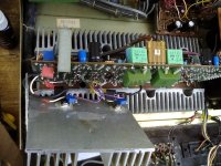
I completed the cascodying of the other channel (one pair of VFETs per channel still) in a much orderly way.
I also experimented the problem with bias current: the other channel, whose bias regulation was working quite well with a 1K pot, now only goes to 5mA. The other channel goes up to about 2mA! Vgs is around 18V for the VFETs. I am trying to understand how this is possible...I will have to try 2K pot and see if that works.
Any thoughts?
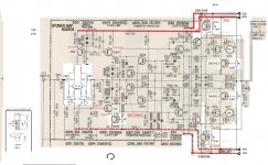
Please consult diagram of the mod above.
Anyway, the cascoded amp sounds very different than the stock amp, based on previous channel analysis on good mono recordings: stock amp sounded very crystalline and transparent but overall on the light side; the cascoded amp is DARK, has very good bass, mid-bass foundation, good bass harmonics, long decays etc (all the attributes that make people say "powerful") and good transients (even at this very low bias) and is non-aggressive, soft sounding, though I miss the crystal clear top of the stock amp. Anyway, with traditional digital sources it complements well. This class B amp sounds very much like some of my class A amps...
I attach pics about the mod. Please see the left upper corner of the complete mod. Note that I am taking signal directly from "Flat Amp" through connector "8".
When I figure out the bias problem, I will probably add the rest of the VFETs and then I will get rid of the tone control board to have space for the addition of -ECdesigns-' "charge-transfer" supply, which I try to use in all my amps. Then connectors and binding posts swap and that would be all for now, I guess...
At the end, I have perfectly stable, dark sounding amp.
Cheers,
M.
The Leach Amp - Output Stage
I completed the cascodying of the other channel (one pair of VFETs per channel still) in a much orderly way.
I also experimented the problem with bias current: the other channel, whose bias regulation was working quite well with a 1K pot, now only goes to 5mA. The other channel goes up to about 2mA! Vgs is around 18V for the VFETs. I am trying to understand how this is possible...I will have to try 2K pot and see if that works.
Any thoughts?
Please consult diagram of the mod above.
Anyway, the cascoded amp sounds very different than the stock amp, based on previous channel analysis on good mono recordings: stock amp sounded very crystalline and transparent but overall on the light side; the cascoded amp is DARK, has very good bass, mid-bass foundation, good bass harmonics, long decays etc (all the attributes that make people say "powerful") and good transients (even at this very low bias) and is non-aggressive, soft sounding, though I miss the crystal clear top of the stock amp. Anyway, with traditional digital sources it complements well. This class B amp sounds very much like some of my class A amps...
I attach pics about the mod. Please see the left upper corner of the complete mod. Note that I am taking signal directly from "Flat Amp" through connector "8".
When I figure out the bias problem, I will probably add the rest of the VFETs and then I will get rid of the tone control board to have space for the addition of -ECdesigns-' "charge-transfer" supply, which I try to use in all my amps. Then connectors and binding posts swap and that would be all for now, I guess...
At the end, I have perfectly stable, dark sounding amp.
Cheers,
M.
Attachments
Last edited:
Completely stable dark sounding amp without proper bias?
There is nothing in the link you referenced about cascoding in output stages, especially not this type you are using (it has nothing whatsoever to do with how the TA-N7 output stage works, by the way). Additionally, because the voltage drop on the BJT is small and the cascoding action occurs within only a very small fraction of the output signal, the voltage swing on the source terminal is negligible, so that kind of cascoding does almost nothing except increase the effective negative Vgs by the voltage drop on the BJT. If it actually did work, it would provide a positive feedback via the source of the VFET. Fortunately, because the VFET has a very low gain (about 5-7) that wouldn't be much and the only effect is really the bias.
The reason you have low bias current is because the (referenced to source) negative bias voltage is now more negative than before (by the BJT voltage drop) for the same setting on the pot, plus the Vds is lower than before (also by the BJT voltage drop). Both make the bias current LOWER. In other words, it seems you do not understand how a VFET works?
Also, the reason the amp is stable may very likely be the absence of bias current. Without it, the transconductance of the output stage is very low and it's not really working around the crossover region, the drivers now have to supply this current. The higher current likely increases the transconductance of the driver stage to a point where gain-bandwidth is sufficiently higher for the compensation to work properly and the amp not to oscillate.
All that being said, if you like the sound, then your mission is a success I suppose, in an 'end justifies the means' way.
Regarding the power supply - if the +44 and +80V (and corresponding negative supplies) do not come up in the proper sequence, fuses will burn - the first couple of times. Do it enough and the VFETs will dies, and no, the BJTs will not save them. They only save them if they fail open and with overcurrent they fail short. This is the main reason why VFETs die in the N7, these BJTs are overstressed in non-obvious ways in that design but they do usually last one or two decades. However, after that... typically they will fail when testing on a curve tracer, if not just show severe degradation.
Last edited:
Dear Ilimzn,
I really appreciate your recommendations and contributions.
I only wish you refrain your urge to tell other people that you suspect other people doesn't really understand what is going on, at each moment.
I get not offense but it is, nevertheless, disturbing...I declare that I understand (vaguely) the principles by which the VFET works and now I have three VFET amps working, but I only now the units for a year or so...that is different to say I understand completely how discrete power amplifiers work, which I don't.
I confess in my rush I did not measure bias voltage (gate-to-gate) for the drivers, with different positions of the pot. I shall remedy this ASAP.
I learn while I do. A reckless approach, I agree, but there is no other way to do it for me...I am very conservative in my real life, though.
Fortunately, the problem with HF is apparently only a question of burn-in, as the highs are coming better by the hour. It has occurred to me previously when using those red Wima caps.
Indeed, the bias is slow, the sound is good and the amp is stable, even when challenging it with the light bulb at power up.
I took the liberty to copy the part of the article that interest us:
"Some correspondents have asked me why I did not use an ouput stage in which the output transistors are operated in the common emitter mode. Such a stage is shown in Figure 6 where the collector of output transistors Q18 and Q19 drive the loudspeaker load. Sometimes this circuit is referred to as a complementary Sziklai connection. Transistors Q14 through Q17 are the driver transistors. Each side of the output stage consists of a common emitter stage (Q14 and Q15) driving a common collector stage (Q16 and Q17) driving a common emitter stage (Q18 and Q19). I have seen some versions of this stage in which Q16 and Q17 are omitted. These transistors provide current gain to drive the bases of the output transistors. Without them, Q14 and Q15 would have to be biased at a high current which would cause them to run hot.
Circuit Diagram (see attachment as it did not copy)
Figure 6. Common-Emitter Output stage.
If the junction between R34 and R35 is not connected to the output lead, the stage would have a high voltage gain, a very low bandwidth, and a very high output impedance. The overall amplifier would oscillate unless the gain of the output stage is reduced. To reduce the gain of the stage, widen its bandwidth, and decrease its output impedance, the junction between R34 and R35 must connect to the output lead. This adds negative feedback to each half of the stage to force it to operate at unity gain. In effect, pre-drivers Q14 and Q15 act as emitter followers to set the output voltage while output transistors Q18 and Q19 supply the load current. Some load current is also supplied by the driver transistors.
The connection of R34 and R35 to the output lead can cause the driver transistors to operate class-AB rather than class-A, which adds to crossover distortion. To see how this occurs, suppose the output voltage is going positive. The current in Q14 is increasing, which causes its base-emitter voltage and the voltage across R34 to increase. Because the VBE multiplier holds the voltage between the bases of Q14 and Q15 constant, the emitter-base voltage of Q15 decreases, causing it to cut off. This cuts off Q17 and Q19. Therefore, the lower three transistors in the output stage cut off. When the output voltage goes negative, the upper three transistors cut off. In the common collector stage of Figure 1, only the output transistors operate class-AB. The four driver transistors all operate class-A.
Because there is a local negative feedback loop around each half of the common emitter output stage, it is susceptible to parasitic oscillation problems which can occur at high frequencies where phase shifts in the two feedback loops can cause the loop gains to become positive. In effect, these phase shifts occur because there is a delay between the time that Q14 and Q15 set the output voltage and the time that Q18 and Q19 supply the output current. This delay is caused by the internal capacitances of Q18 and Q19. Because Q18 and Q19 are connected in the common-emitter mode, the Miller effect causes the internal capacitances to be much larger, thus slowing down the response of the output transistors and increasing the delay in their collector output currents. Because the output transistors have the largest internal capacitances and the lowest gain bandwidth product, it only makes sense to me to operate them in the configuration that they exhibit the widest possible bandwidth. That configuration is the unity gain common collector connection."
Thanks again for your help.
M.
Attachments
The problem is that you keep comparing two things that are different and then somehow concluding the problem is the same, and then going one step further and introducing a cascode as a solution (which is not even mentioned in the text you referenced in any way).
1) How do you know it's the output stage (VFETs) that are oscillating?
2) The Sziklai connection as drawn in your quote is NOT correct (and yes, the Prof does make mistakes). It would be a Sziklai connection if colectors of Q18, Q16 connected to emitter of Q14, and also collectors of Q17, Q19 connected to emitter of Q15 (with appropriate scaling of R34/R35) The way it is drawn. the NFB loop is around BOTH Q14 and Q15.
3) Granted, the driver circuit of the TA5450 is similar in some ways but not the same, it is NOT to be dismissed that the source of the VFET goes from one power supply, and the driver part goes from another. At the very least this means that instead of a 'R45' as on your referenced schematic, there are impedances of a whole lot of withing and two power supplies.
4) Replacing the output BJTs in your referenced schematic with VFETs (including the change to the power supply situation) changes a LOT. A VFET is a completely different beast compare to a BJT. One thing which is wildly different are input capacitances (MUCH smaller), voltage rather than current drive and vastly lower transconductance, and also internal impedance on the order of 10 ohms, not kiloohms like the BJT.
5) VFET is indeed completely different than any other semiconductor in use. It is only notionally similar to a JFET for being depletion mode, but it is not in any way to be approximated with a current source like all other FETs and all BJTs. The current through a VFET depends on voltages on ALL of it's electrodes, and there are no real treshold voltages as such.
6) gate to gate bias is actually fairly irrelevant, what is relevant is gate to source, also source to drain.
I would urge you to first take the schematic of the original 5450 power amp and simply remove the protection parts, to see there is far more going on in that driver, and try to figure out why. This is the key.
Yes, I am aware of what you state. Thank you for pointing me that Vds is also very important. Unfortunately, I cannot make another trafo with higher V to compensate for the consumption of the cascode.
Sorry, I keep making the same mistake. I meant base-to-base voltage between opposite drivers, which I understand bias these to pass current so that +/-76V reduce its value and become the V bias (together with source V), Vgs, for the VFETs. At least that's how I see it.
Removing the protection didn't help. I already tried that.
I don't know what is starting the oscillation, but the whole output section is involved, and the VFETs are at risk. The paper provided a clue to as it can be a case of Miller capacitance doing wrong. Maybe a Colpits resonator? WHo knows...not me certainly.
Anyway, you may think cascodying is no magic but certainly it does something magical to the sound: it just sounds more like music...that is why I was already modifying some of my outputs, because I heard significant imrpovements everytime, not because I am an incurable stuborn...
Someday I will hopefully understand this complex circuit, with your help I hope
Best wishes,
M.
The bias of the VFET comes from base to base difference of Q310/311. However, the result is the actual VFET bias Vgs, and it need not be the same for the P and N part as they are not ideally complementary and do vary quite a bit even within the same rank.
The bias is developed by droping voltage from the +-75V supply with respect to source of the VFET, but consider what this means - any change on the +-75V line and any change at the source (normally +-44V line) changes the bias voltage. Also, any change of the +-44V line changes Vds. Both affect the VFET current. In your case the source voltage is also affected by the output voltage, so one more variable.
Note C310/C313. Have you tried to stop the oscillation by changing values?
Yes. I tried 39pF without success.
Now it is sounding so good that there is no way back. Though I never heard the stock amp in stereo (only mono), I like this sound better. Now not only it has good basement but musical detail and nuances, instrument's textures and colors. all are coming through nicely. Low level detail and ambient sounds are much pronounced, which gives that "live event" impression so welcome.
Now my focus will be to recuperate bias regulation. Given VFET's response curves, with my present Vds, I need much lower Vgs. I will swap some resistances and experiment. The bias pot will be increased to 2K. I can also decrease the emitter resistors for the pre-drivers and see what happens...I bet it will sound more dynamic with that move. I have now higher value for VFETs gate resistors (130R if I remember correctly) that could also influence VFET's behavior, I imagine. Ah! The joys of experimentation and learning.
I even have spare NEC VFETs which I could use on another project for an "all VFET cascode output", as time allows...
Bet wishes,
M.
i have one and just replace all the diodes and capacitors of the amp section.
and remove the input capacitor. . my only concern is the mesure at the bias point . i have 75mv as needed but it is not very stable during the mesure . is there a malfunction somewhere even if it sounds very good
and remove the input capacitor. . my only concern is the mesure at the bias point . i have 75mv as needed but it is not very stable during the mesure . is there a malfunction somewhere even if it sounds very good
i have one and just replace all the diodes and capacitors of the amp section.
and remove the input capacitor. . my only concern is the mesure at the bias point . i have 75mv as needed but it is not very stable during the mesure . is there a malfunction somewhere even if it sounds very good
Congratulations, colleague.
Bias shall be measured after a while when amp is "warm", say 30min or so...then it should not move much, safe if you have signal passing
If I remember correctly, the last recommendation was 50mV.
Enjoy this excellent amp from the 70´s.
M.
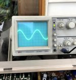
OK, I finally had the time to do some tests.
It happens that my low bias amp doesn't show crossover distortion whatsoever. I tested sine at 4 Watts (the more that my ears bear; I did not found dummy load) and there was a perfect sine on both channels. I imagine that VFETs in this arrangement never go off...
(see example picture; lower power)
I also reduced the voltage consumption of the common-base cascode BJT to only 4V.
Vgs is now around 16.5V for the VFETs. Bias is 6ma!
Now I will begin listening tests.
I only tested music until around 25Watts and it did not clip.
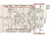
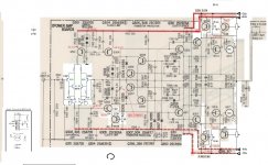
I attach a concept schematic (not a finished one; probably contains a lot of errors) of the modded 5650, based on the several discussions about "thermal memory distortion" going around. I plan to test some of these on my amp. Who nows, perhaps I end with a "memoryless" amp...I particularly like the cascoded drivers which would allow tight control of the bias voltage for the VFETs, which in my case should be lower, and even allow the possibility of using another different power supply, other VFETs or make a clone amp...apart the known effects of this strategy.
Cheers,
M.
It happens that my low bias amp doesn't show crossover distortion whatsoever. I tested sine at 4 Watts (the more that my ears bear; I did not found dummy load) and there was a perfect sine on both channels. I imagine that VFETs in this arrangement never go off...
(see example picture; lower power)
I also reduced the voltage consumption of the common-base cascode BJT to only 4V.
Vgs is now around 16.5V for the VFETs. Bias is 6ma!
Now I will begin listening tests.
I only tested music until around 25Watts and it did not clip.
I attach a concept schematic (not a finished one; probably contains a lot of errors) of the modded 5650, based on the several discussions about "thermal memory distortion" going around. I plan to test some of these on my amp. Who nows, perhaps I end with a "memoryless" amp...I particularly like the cascoded drivers which would allow tight control of the bias voltage for the VFETs, which in my case should be lower, and even allow the possibility of using another different power supply, other VFETs or make a clone amp...apart the known effects of this strategy.
Cheers,
M.
Attachments
To keep this thread updated, I copy the mod posted on my other thread about "thermal memory":
"OK. I know have the input section of my Sony TA-5650 properly modified with Peufeu's Cascoded CFP trick (see diagram on previous post). The effect was easily detected as being the same caused on the Blame. Less aggressive highs, more midrange presence (the bodies of the instruments are very pronounced), better delineation of melodic lines, in all, if I knew how to speak Latin, I would say the sound is now rotundum
Fortunately, the DC offset was low and I had not to mod the circuit: 10mV and 1,8mV."
This is the thread:
http://www.diyaudio.com/forums/soli...p-amplifier-gentleman-memory.html#post5355159
I had a little difficulty in fitting the units in the existing space for the differential pair. I had to desolder some film caps and the re-solder them.
Very worthwhile mod.
Cheer,
M.
Attachments
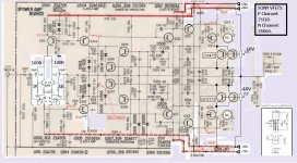
I see that my vertical cascade of the output elements, while providing me a stable amp to enjoy, is technically wrong or far from optimal.
I plan to mod it as follows (see attachment), as time and my Amnesis amp project allows. That would be, IMHO, a proper cascoded common-source output for the VFETs, maintaining the original bias, hopefully...
(please ignore the driver's mod)
Cheers,
M.
I plan to mod it as follows (see attachment), as time and my Amnesis amp project allows. That would be, IMHO, a proper cascoded common-source output for the VFETs, maintaining the original bias, hopefully...
(please ignore the driver's mod)
Cheers,
M.
Attachments
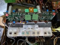
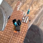
Now that my Amnesis experimental amp project is on its final state, I can update.
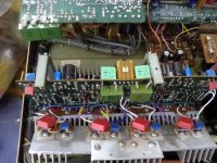
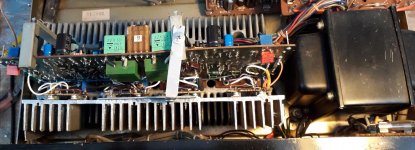
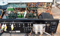
Here, some pics about the present state of the SONY TA-5650, while I rest and plan the next move--> use big power devices (BJT or MOSFETs) instead of that little BJTs, cascodying the VFETs at higher V reference point, "closer" to the VFETs.
With the present arrangement, normal current biasing is possible. No oscillation whatsoever...
Cheers,
M.
Attachments
Last edited:
- Status
- This old topic is closed. If you want to reopen this topic, contact a moderator using the "Report Post" button.
- Home
- Amplifiers
- Solid State
- My Sony TA-5650 VFET amp adventure.