Happy new year!
Have a look here:
2stageEF high performance class AB power amp / 200W8R / 400W4R
@Dave: have you officially released your simulation models to the community? Many thanks for your help designing the IXYS MOSFET based amp in the link above!
BR, Toni
Have a look here:
2stageEF high performance class AB power amp / 200W8R / 400W4R
@Dave: have you officially released your simulation models to the community? Many thanks for your help designing the IXYS MOSFET based amp in the link above!
BR, Toni
@Dave: have you officially released your simulation models to the community? Many thanks for your help...
I still haven't fully checked them but I am happy to share them, or for you to do so.
It was a pleasure to help, I believe I read that you plan to build 4 more channels of the amp, once your lab and home theater are finished.
Nice home improvement, and nice to have the model work put to use.
Best wishes
David
Short inputs to ground.
Place two AC sources in series with feedback after loading an amp.
Draw a plot for an equation shown ...
Hi Pavel and David,... "virtual transformer" that extracts the common mode and differential mode ... When the inputs and outputs are placed correctly then it can be used to measure both common mode and differential mode Return Ratio ...
thank you for the explanations. Looking again at the first two plots in post #1, it seems that Paul used the "cheater" method for loop gain evaluation.
Either way, it is fascinating. Everybody has a special "sub hobby", and it is fun to understand at least roughly what the others are doing in the next room.
")
Happy new year!
Matthias
Progress Update
Thank you everyone for the comments. It's good to have interest from others.
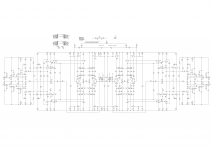
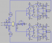
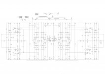
Have processed the information and acted on some of it. Although have been quiet been busy in the background. Have laid out two PCBs. One IPS and one OPS. They have been sent off to a Chinese PCB house just in time to get them made before the Chinese new year.
The basic design is as per attachment except the OPS PCB has been laid out for the LT1166. This is not a final decision but at least allows some basic evaluation. Have not decided what biasing method will be used in the final version. Could be a Vgs multiplier with a Vbe multiplier.
The big IXYS MOSFETs look interesting. Paralleling two pairs of those with independent temp compensation may be looked at. Just wondering how to drive them. Push pull drivers?
As per previous discussion I have been using BesPav's method but now have moved to David Zan's method. There is a discrepancy between the two. BesPav's gives a more "conservative" if less accurate result.
I would like to be able to simulate two differential loops at the same time but my understanding is not great enough to get it to work. It complains about floating nodes....?
Would like to optimise the loops in preparation for the first prototype build. Probably some non obvious issues hidden in the design.
Attached are a few items that may be of interest
Take care,
Paul
Thank you everyone for the comments. It's good to have interest from others.
Have processed the information and acted on some of it. Although have been quiet been busy in the background. Have laid out two PCBs. One IPS and one OPS. They have been sent off to a Chinese PCB house just in time to get them made before the Chinese new year.
The basic design is as per attachment except the OPS PCB has been laid out for the LT1166. This is not a final decision but at least allows some basic evaluation. Have not decided what biasing method will be used in the final version. Could be a Vgs multiplier with a Vbe multiplier.
The big IXYS MOSFETs look interesting. Paralleling two pairs of those with independent temp compensation may be looked at. Just wondering how to drive them. Push pull drivers?
As per previous discussion I have been using BesPav's method but now have moved to David Zan's method. There is a discrepancy between the two. BesPav's gives a more "conservative" if less accurate result.
I would like to be able to simulate two differential loops at the same time but my understanding is not great enough to get it to work. It complains about floating nodes....?
Would like to optimise the loops in preparation for the first prototype build. Probably some non obvious issues hidden in the design.
Attached are a few items that may be of interest
Take care,
Paul
Attachments
Last edited:
Thank you everyone for the comments. It's good to have interest from others.
Have processed the information and acted on some of it.
Paul
That is quite close to what I was talking about, but again I have to say that reading a low resolution jpeg is quite meaningless.
Comments to the H bridge IPS.
There is no need to cascode the cascode.
You can also remove (most, maybe all) of the resistors in the collectors in the H-bridge.
All the best
Reodor
I checked the IXYS brochure and found the devices with the lowest capacitance per amp of useful current capacity.
Hi, Dave!
Let me suppose, that we could remove significant capacitance by cascoding OPS devices.
So, we can use cheap as dirt IRFP140/240's or transconductance-matched FQA36P15/FQA28N15 pair.
And, of course, try simpler drive stage.
Attachments
Hi mlloyd1,
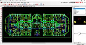
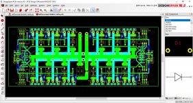
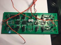
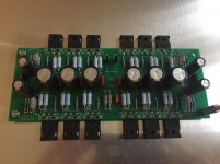
As requested an update. Not too much spare time but have made some progress. Have populated the IPS PCB and debugged it. having found that Farnell had labelled some of the component bags incorrectly. The BC546 were labelled as BC556 and vice versa along with some of the MELF resistors. Lesson learnt, never make assumptions. If it wasn't for this misfortune the PCB would have worked first time. Shows that LTSpice is pretty accurate. So now onto completing the OPS PCB i.e. soldering the drivers and completing the temporary metal work. First run will be without any biasing (LT1166).
Here are a couple of pics. Not the best quality but will give you an idea of what I'm making
Bespav,
Your circuit looks interesting. I keep looking at cascode OPS. Could use one on this design. The amount of voltage swing available even after taking into account the loss due to the cascodes would be more than adequate. But so far in simulations have yet to see any significant advantage. That's not to say there isn't any just nothing I have seen in my limited experience.
Paul
Attachments
Last edited:
- Status
- This old topic is closed. If you want to reopen this topic, contact a moderator using the "Report Post" button.
- Home
- Amplifiers
- Solid State
- Fully Differential Amplifier With CMCL