Hi Sreten,
I've had private e-mails from readers who do understand what I write.
That they don't post on this string is, sadly, down to the way you and Millwood have already treated me.
____________________________________________________
Hi lineone,
The diyAudio link I could not remember the other day was by Steven. See;-
http://www.diyaudio.com/forums/show...2339#post282339
See post#1 for the elongated current waveforms that can be generated.
This means that whichever output half is conducting will run up to the driver or current limit, whilst the other output half still remains in conduction.
This is less efficient than class-B, and could lead to an increase of storage effects at high frequency high power output due to lack of pull-down of a previously conducting output half, but it is considerably more efficient than class-A.
The conduction crossovers occur as with a conventional class-A, ie. no discontinuities or abruptness.
The only disadvantage I can see is that the natural impedance of the output stage is more reliant on NFB than if it were pure class-A, but I would think the difference would not be noticeable as long as not too much advantage was taken of the design.
See the circuit shown in post#11.
____________________________________________________
There is also 'd2s' amplification which was expanded upon in two Electronics World articles.
____________________________________________________
My own 100W 8 ohm class-A project has a similar output conduction waveform to fig #1 with quiescent dissipation equalling the maximum class-A output (150W), but for impedance dips it goes beyond that into class-AB so that output transistor base charges can dissipate for full frequency range at lower impedance. The A-B conduction crossover is very gradual though.
Still in prototype form, and will not be released until I am sure of every performance aspect, like temperature, supply variation, etc.
I never report anything that I do not have direct experience of.
Cheers for now ........... Graham.
Graham,
Now that you have wetted our appetites, how about posting a conceptual of your 100 watter......")
http://www.superlaugh.com/1/bluechicken.htm
Regards,
Jam
Now that you have wetted our appetites, how about posting a conceptual of your 100 watter......
http://www.superlaugh.com/1/bluechicken.htm
Regards,
Jam
Hi Linesource,
Another circuit to consider is Douglas Self's Trimodal design.
It can be adjusted to run in class-A up to a pre-determined level after which it automatically becomes class-AB. This circuit has an output bias regulator which obviates any need for thinking about output device gain characteristics, other than complementary matching.
Some people do not like the sound of Self's amplifiers, but if you organise VAS collector to differential NFB base feedback and remove the series output choke you can get rid of Miller C.dom induced propagation delay which increases crossover induced distortion when load currents are out of phase with the voltage drive, also get rid of mid-bass loudspeaker back emf induced artifacts that generate additional tweeter noise.
You could easily set up 25W class-A for your very low first Watt distortion, and then design for much more output in class-AB with the switching crossover occuring at levels where its effects are not going to be a problem.
Cheers ........... Graham.
Hi Linesource,
I know your original request was for class-A, which obviates any risk of crossover distortion and gives a more naturally low output impedance, but there are alternatives.
also jcx and jam are following this thread so I am including two other circuit variants could be further developed.
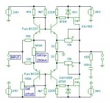
Attached here is a 'd2s' ( difference of two squares ) circuit due to Ian Hegglun as published in Electronics World + Wireless World in Sept 1995, page 753.
Redrawn to avoid copyright problems. I do not know if there are any patents pending.
It is a class-AB square law circuit that has a long based and very gradual curvilinear crossover characteristic. An open loop distortion of 0.3% is quoted for 10kHz at 8 ohms, and thus a single driving IC could easily reduce distortion to 0.001%. 50W average was proposed, but output shown only with 22V rails.
There has never been any follow-up to this simple design, though Ian also published a more complex version with IC and bipolar outputs, but it used two pairs of complementary mosfets to generate the curvilinear crossover.
Back soon .............. Graham.
I know your original request was for class-A, which obviates any risk of crossover distortion and gives a more naturally low output impedance, but there are alternatives.
also jcx and jam are following this thread so I am including two other circuit variants could be further developed.
Attached here is a 'd2s' ( difference of two squares ) circuit due to Ian Hegglun as published in Electronics World + Wireless World in Sept 1995, page 753.
Redrawn to avoid copyright problems. I do not know if there are any patents pending.
It is a class-AB square law circuit that has a long based and very gradual curvilinear crossover characteristic. An open loop distortion of 0.3% is quoted for 10kHz at 8 ohms, and thus a single driving IC could easily reduce distortion to 0.001%. 50W average was proposed, but output shown only with 22V rails.
There has never been any follow-up to this simple design, though Ian also published a more complex version with IC and bipolar outputs, but it used two pairs of complementary mosfets to generate the curvilinear crossover.
Back soon .............. Graham.
Re: Gain?
Hi Elso.
I'm not Graham...but the open loop gain, of each alf of the circuit he gives ,is ,in the second BC 337 the relation between is colector and emitter resistors... 220/33 =6,7
More the gain of the output mosfet that has a transconductance of 1 S (1A/Volt)...that gives for the mosfet with a 8 ohms load a gain of 8X.
The gain of each half in then 6,7 X 8 =53,6 .
Jorge
Elso Kwak said:where is the gain in the circuit you posted?
Hi Elso.
I'm not Graham...but the open loop gain, of each alf of the circuit he gives ,is ,in the second BC 337 the relation between is colector and emitter resistors... 220/33 =6,7
More the gain of the output mosfet that has a transconductance of 1 S (1A/Volt)...that gives for the mosfet with a 8 ohms load a gain of 8X.
The gain of each half in then 6,7 X 8 =53,6 .
Jorge
It's unclear to me why you'd use MOSFETs to drive a 1R load, either. For something like that, you want the lowest sat voltage and the highest gm you can get your hands on, and that means bipolars. Heck, you might even think about germanium!
The question of back EMF is just as mystifying to me, since as far as I know, resistors don't generate back EMF.
The question of back EMF is just as mystifying to me, since as far as I know, resistors don't generate back EMF.
Hi Aksa,
Thank you for your calming influence.
I merely pass on the thinking I now apply to amplifier design. At one time I too applied a low voltage headroom with bipolars, but I no longer design 'audio frequency' amplifiers for simplistic resistor loads, I go straight to a loudspeaker driving 'audio' amplifier. It is designing for steady state sinewave driven zero phase resistor load testing that has until quite recently left us with a plethora of 'audio frequency' amplifiers that will never drive loudspeakers satisfyingly.
I had my grounding with valve amps, ultralinear KT88s - which are now making a comeback, and it was these that made me seek out the weaknesses within solid state 'replacements'. Quite literally it has taken me three decades; this all because I believed what the early designer 'experts' said I should.
I don't mind the questions at all, it keeps everyone on their toes. Also they make me realise where further explanation and/or investigation might be required.
It is only when an understanding dawns about what I said about the 5V headroom with regard to high frequency bipolar slewing with a loudspeaker load that causes a momentarily increased draw of out of phase current which has not actually been expected, that this simple expediency can be seen to help the output devices. I now closely observe all inner amplifier nodes and device current paths whilst simulating with representative loudspeaker loads, NOT JUST a 4 or 8 ohm resistor. The problems simply DO NOT show with steady sinewaves and resistor loads ! So called <0.01% THD figures are often worthless.
Thanks for saying that you do not always agree, and feel free to question in case I might mislead anyone or if I post an erroneous statement. Calm discussion and debate are always worthwhile.
Cheers ........... Graham.
Hi Tube Dude,
Its not my circuit, but I read it the same as you.
The 10k pots from output back to the 330 ohm emitter resistors were also a local NFB. I believe the gain was individually set for each half for 1.5V input, and monitored by observing input and output straight line linearity with a triangular waveform.
Maximum sinewave efficiency was quoted as 64%.
The input bipolar pairs set up an exponential crossover at low amplitude - this is very gradual.
Cheers............. Graham.
I'm baffled.
I still don't know why 25 W class A into 1R is required, seems an
obvious question to me. If its a ribbon tweeter then a transformer
is the the sensible option, if its a speaker then 1R doesn't make
any sense at all, it could be easily rearranged for higher impedance.
The general musings on "the best way to build an amplifier" have
serious consequences for a low voltage low impedance load class
A amplifier in a way which they wouldn't for 25W class A into say
4 or 8 ohms.
But who cares about such technical trivialities.
sreten.
I still don't know why 25 W class A into 1R is required, seems an
obvious question to me. If its a ribbon tweeter then a transformer
is the the sensible option, if its a speaker then 1R doesn't make
any sense at all, it could be easily rearranged for higher impedance.
The general musings on "the best way to build an amplifier" have
serious consequences for a low voltage low impedance load class
A amplifier in a way which they wouldn't for 25W class A into say
4 or 8 ohms.
But who cares about such technical trivialities.
sreten.COMPLEMENTARY DIFFERENTIAL
Here is a summary of the thread ideas so far
1) Bipolar transistors are best to drive 1 ohm output resistance
2) 25 watts into 1 ohm can be obtained with a low +/- 8-10 volts output supply
3) low voltages = low voltage gain and hgh current gain input stages
4) bipolar input and driver stages would be better than JFET or MOSFET with low voltage rails
5) complementary differential topology can reduce 2nd harmonic
6) cascode current sources will offer lower distortion than resistors
WILL THIS WORK? WHAT CHANGES NEEDED? ANY BETTER CKTS?
Attachments
Linesource.
Pretty complicated circuit. I am sure you could simplify it or maybe not.( You probably don't need the cascodes on the diff. pairs)
I would use a triple darlington for the output. Charles Hansen pointed this out and information on the triple is available on the Marshall Leach web site.
Regards,
Jam
Pretty complicated circuit. I am sure you could simplify it or maybe not.( You probably don't need the cascodes on the diff. pairs)
I would use a triple darlington for the output. Charles Hansen pointed this out and information on the triple is available on the Marshall Leach web site.
Regards,
Jam
Hi Linesource,
As sreten has asked, I do not know what kind of load, and what frequency range you intend driving ??
That circuit is complex and can be set up for your 25W class-A, but would run into class-AB beyond, with possible conduction crossovers if there are phase shifted impedance dips.
This would mean ensuring that the value of the Miller connected VAS C.doms are not too high. If the amp never crosses into class-B then forget that comment, but it could do so with dynamic loudspeaker loading from what might be the equivalent of a much lower than expected output level when compared with resistor examination. This relates to my earlier comment with the D Self design.
The complementary amplifier halves will have different dynamic gain characteristics at high audio frequencies which will require different degrees of error correction. When the NFB loop is shared back to both input stages with the same R/C+R or R/R divider, the ouput driver bases -might- be better tied together with a capacitor across the bias network to limit high frequency differential current generation through the output devices wrt the output node.
Zeners at the current sources would prevent output bias drift with unregulated supply line variation.
The differential mirror transistors will NFB error correct much more quickly if they have more millivolts of Vce, as with a LED//10nF in series with bases; are cascoded mirrors running at Vbe really better for hf resolution ? Maybe more accurate at dc, but personally I don't think better for coherent NFB control.
The VAS transistors may be susceptible to momentary overload saturation and are emitter degenerated; Cs are noted but values and currents are not shown. Emitter degeneration increases the effect of internal Cbc + ext Miller at that stage which slows down the amplifier's ability to error correct loudspeaker induced back emfs through load induced crossover distortion. The VAS collector becomes slowed down as it tries to 'switch' through the output bias class-B crossover range and thus error is created; I don't know your load though.
I can't help thinking that something more simple such as Jos's ESL proven amplifier would be more transparent with real audio signals and real loudspeakers. The JLH circuit has never had most of the disadvantages that arise in many other designs.
Cheers ................. Graham.
Re: COMPLEMENTARY DIFFERENTIAL
There are probably simpler circuits, is depends how you
approach the "sometimes less is more" philosophy.
Just some notes from reading D. Selfs book:
a) A triple EF is probably best for avoiding parasitic oscillation
in the output stage.
Classic Darlington connection is simply dismissed as "ill-advised".
A triple CFP is probably best for avoiding 3rd harmonic distortion
at high current, but parasitic oscillation is apparently a very big
problem with triples.
b) To optimise output swing a CFP stage is needed.
An EF stage needs an extra 0.6V per rail, a triple another 0.6 V.
Low value emitter resistors also keep up voltage swing.
Depending on the driver stage and output topology output swing
will be ~1 V to ~3V below each rail, the circuit you show is ~3V.
If correctly dimensioned rails are used the output stage will
never leave Class A operation, if the the rails are higher more
static power is dissipated, and power output will improve,
but at the cost of the output stage leaving Class A operation.
So your choice is Class A all the way or moving into A/B near
clipping levels, the voltage rails need to be carefully chosen.
(this is all presuming a pure 1R resistive load)
Running the driver stage with higher rails will not help,
you state that these are to be regulated, so obviously
you will need a separate higher voltage rail for this,
to allow for the working voltage of the regulators.
c) In the less is more vein, some argue (and I agree) that
fully symmetrical design is a waste of effort. When it is only
effectively canceling small amounts of 2nd harmonic leaving
3rd untouched some would rather keep the 2nd and instead
concentrate on reducing the 3rd, i.e. reduce overall distortion.
Single ended design for parts of the amplifier is certainly easier.
d) do the current sources really need to be cascoded ?
(Less is more mentality again)
They look like they'd work better in an IC as is,
I think some emitter resistors are needed.
e) As GM alludes to, what D.Self calls an EF type II with
a "speed up" capacitor will improve high frequency swing.
(Though Class A operation obviates its major advantage,
but if you have AB near clipping it seems a very good idea.)
f) If the load is not 1R pure resistive things get much more
complicated and a very good solution has another whole
set of problems to consider.
g) Sometimes the simplest (but technically sound) is
the better approach compared to more complex circuitry.
sreten.
LineSource said:Here is a summary of the thread ideas so far
1) Bipolar transistors are best to drive 1 ohm output resistance
2) 25 watts into 1 ohm can be obtained with a low +/- 8-10 volts output supply
3) low voltages = low voltage gain and high current gain input stages
4) bipolar input and driver stages would be better than JFET or MOSFET with low voltage rails
5) complementary differential topology can reduce 2nd harmonic
6) cascode current sources will offer lower distortion than resistors
WILL THIS WORK? WHAT CHANGES NEEDED? ANY BETTER CKTS?
There are probably simpler circuits, is depends how you
approach the "sometimes less is more" philosophy.
Just some notes from reading D. Selfs book:
a) A triple EF is probably best for avoiding parasitic oscillation
in the output stage.
Classic Darlington connection is simply dismissed as "ill-advised".
A triple CFP is probably best for avoiding 3rd harmonic distortion
at high current, but parasitic oscillation is apparently a very big
problem with triples.
b) To optimise output swing a CFP stage is needed.
An EF stage needs an extra 0.6V per rail, a triple another 0.6 V.
Low value emitter resistors also keep up voltage swing.
Depending on the driver stage and output topology output swing
will be ~1 V to ~3V below each rail, the circuit you show is ~3V.
If correctly dimensioned rails are used the output stage will
never leave Class A operation, if the the rails are higher more
static power is dissipated, and power output will improve,
but at the cost of the output stage leaving Class A operation.
So your choice is Class A all the way or moving into A/B near
clipping levels, the voltage rails need to be carefully chosen.
(this is all presuming a pure 1R resistive load)
Running the driver stage with higher rails will not help,
you state that these are to be regulated, so obviously
you will need a separate higher voltage rail for this,
to allow for the working voltage of the regulators.
c) In the less is more vein, some argue (and I agree) that
fully symmetrical design is a waste of effort. When it is only
effectively canceling small amounts of 2nd harmonic leaving
3rd untouched some would rather keep the 2nd and instead
concentrate on reducing the 3rd, i.e. reduce overall distortion.
Single ended design for parts of the amplifier is certainly easier.
d) do the current sources really need to be cascoded ?
(Less is more mentality again)
They look like they'd work better in an IC as is,
I think some emitter resistors are needed.
e) As GM alludes to, what D.Self calls an EF type II with
a "speed up" capacitor will improve high frequency swing.
(Though Class A operation obviates its major advantage,
but if you have AB near clipping it seems a very good idea.)
f) If the load is not 1R pure resistive things get much more
complicated and a very good solution has another whole
set of problems to consider.
g) Sometimes the simplest (but technically sound) is
the better approach compared to more complex circuitry.
sreten.I would go with a simpler circuitry, like those pass class a designs (aleph for example).
I would also go with a bjt design as well for dissipation purposes. the problem with the jlh is that it doesn't do too well with capacitive loads: I tried an experiment paralleling a 1uf cap to a 8ohm load and the highers were muffled on the (bjt) jlh.
my mosfet version doesn't suffer from that at all. But it would have severe dissipation problems driving 1ohm load because of mosfet's high "saturation' voltages (unlike indicated by graham earlier, BJTs have very low saturation voltages). so from that point of view, bjts have a considerable advantage over mosfets in this particular application.
the IRL3103 mosfet i used in my sim earlier in this thread has lower on voltage than most suitable bjt at the ~6-8 A that you might use in this amp (and that’s looking at ic/ib = 10 bjt saturation curves)
the gate drive V requirement is well within the typical op amp +/-15 V supply capability - one of the first steps in amp performance improvements is to use a separately regulated, higher voltage supply for the input/predriver stages of an amp
the actual gate current in my sim is ~0.5 mApp, i used 50 mA bias to get low Z and max bandwidth from the driver transistors (and in anticipation of seriously large, nonlinear gate drive requirements to recover from saturation)
so i believe that mosfets are contenders - even preferable in this application
- Status
- This old topic is closed. If you want to reopen this topic, contact a moderator using the "Report Post" button.
- Home
- Amplifiers
- Solid State
- best topo for 25W class A into 1 ohm resistive load?