It seems like there should be some way of measuring the problem. It appears the physical circuit deviates a little too much from the model. It should be possible to open the feedback loop and look at the operation of each stage in progression. Or maybe open the amplifier circuit and drive the output stage with a low distortion amp. See what it's doing and how much it deviates from the model. Somehow, I usually tend to have a philosophical preference for tracking down a problem rather than speculatively trying things without first understanding what's wrong.
On the other hand if you know an easy fix is likely to work, it can sometimes be a lot faster to try it before getting too analytical.
On the other hand if you know an easy fix is likely to work, it can sometimes be a lot faster to try it before getting too analytical.
Last edited:
Okay - 5W Rev 2 design files and 10W Rev 1 design files.
Biggest difference between the Rev 1 and rev 2 layout is that I've been a little more careful with the ground connection to the feedback divider. The original ground pour did nothing to preserve distortion performance, and may be responsible for some of the mediocre performance into 8Ω.
Size is 77x36 for the 5W variant, and 99.5x36 for the 10W one.
Of course there's also the changes to the schematic with the current loads for stage 1, improved compensation, doubled-up current sink/source for the drivers etc., but they're explained above.
Alas we're just about to hit Chinese new year, so I doubt I'll be getting these PCBs to play with for a good few weeks
Attachments
Found the culprit.
<Happy Dance>.
It's a rookie mistake on the feedback network layout. Rather than sampling at the point where the load connects to the PCB, I'm sampling at the other end of the trace, simply because it's nearest the amp input. So of course the amp has gobs of even order harmonic distortion as the load current goes up - the PCB traces are messing with the feedback ratio.
I've corrected the prototype PCB by cutting the link between the feedback resistor and the pour for output, and inserting a length of wire wrap wire to connect the feedback resistor directly to the output pin.
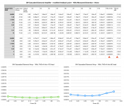
Distortion levels into 8Ω are much improved - I get a minimum of 2.4ppm at 2.5V (0.78W). I'm running into clipping a little earlier than I was previously - I think I might have been mucking around reducing output stage quiescent currents on this amp, so I can probably improve on the 2.4ppm number. See attached plot.
<Happy Dance>.
It's a rookie mistake on the feedback network layout. Rather than sampling at the point where the load connects to the PCB, I'm sampling at the other end of the trace, simply because it's nearest the amp input. So of course the amp has gobs of even order harmonic distortion as the load current goes up - the PCB traces are messing with the feedback ratio.
I've corrected the prototype PCB by cutting the link between the feedback resistor and the pour for output, and inserting a length of wire wrap wire to connect the feedback resistor directly to the output pin.
Distortion levels into 8Ω are much improved - I get a minimum of 2.4ppm at 2.5V (0.78W). I'm running into clipping a little earlier than I was previously - I think I might have been mucking around reducing output stage quiescent currents on this amp, so I can probably improve on the 2.4ppm number. See attached plot.
Attachments
Good catch, Suzy. 
Can you please show photo of the "white wire" mod?
Btw, I still have not been able to find a BOM, is it part of the design files above but in some proprietary format? About to place an order with Mouser so thought I should throw all these bits in.
Thanks,
X
Can you please show photo of the "white wire" mod?
Btw, I still have not been able to find a BOM, is it part of the design files above but in some proprietary format? About to place an order with Mouser so thought I should throw all these bits in.
Thanks,
X
Good catch, Suzy.
Can you please show photo of the "white wire" mod?
Btw, I still have not been able to find a BOM, is it part of the design files above but in some proprietary format? About to place an order with Mouser so thought I should throw all these bits in.
Thanks,
X
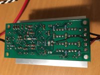
Done, though I've used a black wire. Also shown is the dodgy glob of solder needed where I forgot to connect a couple of pads.
I've exported the BOM to excel format (from Apple Numbers format), and attached that.
Attachments
I've given a quick read to the thread.
What is going on in a diamond buffer is not widely understood. A log(x) voltage drop in signal path gives distortion products "d" proportional to "x" amplitude, the slope of the function is curved. A log(x)-log(K-x) voltage drop in signal path gives distortion products "d1-d2" that cancel out for moderate amplitudes. The diamond buffer cancels out the open loop distortion given by the Ic=K*log(Vbe) nature of Bipolar Junction Transistors. The log(x) function in Vbe comes from physics/chemistry of atoms and electrons, so it is of same nature as universal constants.
This becomes more relevant when there are miller capacitances into play, as it is the Vbe/Ic law of BJT what governs at HF, as soon as the current through capacitances is higher than base current. Early voltage and hFE non-linearity is only relevant when base current is higher than capacitance current. In the old days these miller capacitors were sometimes thrown at the circuits, not for linearization, but just for plain oscillation removal.
I'm going to make some recommendations:
- Mix the diamond buffer of predriver+driver with a CFP of driver+output. This has some advantages. The current from the driver emitter (with less phase shift) still feeds the output of amp while the output transistor turns on. Turn off is different, it is governed by fall time of Ic tail. In a higher power amplifier model, for audio use, there is no need for 1Mhz power bandwidth, of very fast rise times in square waves, just low distortion (and low zero-cross switching EMI, also alleviated/helped by back-emf of series inductor). In the CFP the drivers operate with far less swing of Vbe to correct by predriver stage (diamond).
- Analyze the feasibility of connecting miller capacitors to output lead (instead of pre-drive) in the combined diamond and CFP output circuit.
- Analyze the feasibility of op-amp input stage in higher power models, driving the VAS through cascodes. Analyze feasibility of HF feedback from output of amplifier to output of op-amp, this has current feedback phase margin at HF (less stages lagging for "IN-").
- Take a look at SMD duals: MMDT3904, MMDT3906, MMDTA42 and the like, also NPN/PNP combo. Some are SOT-23-6, some SC-70-6 (SOT-363). These are not useful for all types of stages due to the limited dissipation, but have inherent thermal coupling of pairs, as for current mirrors or LTP biased to few mA.
- MELF is somewhat more expensive and harder to source, unless surplus stock is being put into use. 0603, 0805, 1206 are standard sizes (65mW, 125mW, 250mW). There are also low cost duals and quads, for caps and resistors.
- The pain of MOSFET is transfer function is quadratic: Id=K*Vgs^2. K is quite different for P/N-ch. The class AB driving wave looks like half "circle" instead of half "sine". Good as switches.
Last edited:

Ic=K*log(Vbe) ?? hum...rather ibase=f(Vbe) and ic=f(ibase) in linear region and
ibase=k* exp(Vbe/Vt) and hence ic=k*exp( Vbe/Vt)
from a more detailled discussion can follow there is an optimum of generator resistance for which the non linearity of ic=f(ib) and ic=f(Vbe) reduce to a minimum.
ibase=k* exp(Vbe/Vt) and hence ic=k*exp( Vbe/Vt)
from a more detailled discussion can follow there is an optimum of generator resistance for which the non linearity of ic=f(ib) and ic=f(Vbe) reduce to a minimum.
Congratulation for this very good and useful input. Rare in this forum: Respect.I've given a quick read to the thread....
Specially "Analyze the feasibility of connecting miller capacitors to output lead" that i use now in all my power amps designs since decades.
Elsewhere, the load of the miller capacitance's impedance is not insignificant.
Happy too to see Lazy Cat here, too lazy in his threads ;-)
Last edited:
such was elaborated in detail in an 1983 article ( in German ) and further analysis of NDFLs , lead lag compensation , "Bode compensation" ( 9 dB slope) and why to avoid replacement of resistors with CS ( dynamic distortion).I
- Analyze the feasibility of connecting miller capacitors to output lead (instead of pre-drive) i
Ic=K*log(Vbe) ?? hum...rather ibase=f(Vbe) and ic=f(ibase) in linear region and
ibase=k* exp(Vbe/Vt) and hence ic=k*exp( Vbe/Vt)
from a more detailled discussion can follow there is an optimum of generator resistance for which the non linearity of ic=f(ib) and ic=f(Vbe) reduce to a minimum.
This is a totally flawed way of looking at it, the Ic vs Vbe relationship is fundamental whether beta is 1 or beta is 10,000 it still holds.
but it is exponential not logarithmic. For further enlightenment on semiconductors for ex http://aries.ucsd.edu/NAJMABADI/CLASS/ECE65/12-W/Slides/ECE65_W12-BJT.pdf is recommended. There is no fundamental ic vbe relationship. Cannot be. That is just semiconductor physics.This is a totally flawed way of looking at it, the Ic vs Vbe relationship is fundamental whether beta is 1 or beta is 10,000 it still holds.
The cancellation of the log/exp behavior of BJT (and Si PN diodes), between devices of similar construction, is so dependable that in a LM13700 VCA only +/-2% tolerance in gain between different samples is observed, taking samples of 2 different ages and factories.
[This is: using linearizing diodes for a logarithmic current-to-voltage 1st conversion, then the LTP for an exponential voltage-to-current 2nd conversion. The side of the diodes feeding the LTP is loaded with a current mirror for maximizing usable input range (datasheet shows resistor loading which is far less linear). This is universal scheme for BTJ linearization in variable gain open loop amplification (BJT VCA). The ratio between diode bias and LTP bias controls gain linearly (derivative of log/exp is still log/exp, allowing the shift in operating point to work as gain variation). Drift with temperature is mostly cancelled too, I have measured about 4% for a 50C step in all samples, this is mostly the drift in the current source I use for the diodes.)]
[This is: using linearizing diodes for a logarithmic current-to-voltage 1st conversion, then the LTP for an exponential voltage-to-current 2nd conversion. The side of the diodes feeding the LTP is loaded with a current mirror for maximizing usable input range (datasheet shows resistor loading which is far less linear). This is universal scheme for BTJ linearization in variable gain open loop amplification (BJT VCA). The ratio between diode bias and LTP bias controls gain linearly (derivative of log/exp is still log/exp, allowing the shift in operating point to work as gain variation). Drift with temperature is mostly cancelled too, I have measured about 4% for a 50C step in all samples, this is mostly the drift in the current source I use for the diodes.)]
Last edited:
Technology of integrated amps with bipolars is different from discrete . Moreover in the hi time of TIM debate some French author demonstrated with solide measurements avoid current sources by all means as these make slew rate distortion. ("dynamic distortion"). That has to do with second order semiconductor effects. The effect is basically frequency- and amplitude variable open loop gain. Another article hit the same target "an ultra low noise buffer with gain" showing the the lowest noise is achieved not at all with low noise small signal BJT but with particular CRT drivers. These - now dicontinued- CRT BJT are also the best choice for CS. Leach published an article in Audio Feb 1976 about Low Tim amp - no current sources
Technology of integrated amps with bipolars is different from discrete . Moreover in the hi time of TIM debate some French author demonstrated with solide measurements avoid current sources by all means as these make slew rate distortion. ("dynamic distortion"). That has to do with second order semiconductor effects. The effect is basically frequency- and amplitude variable open loop gain. Another article hit the same target "an ultra low noise buffer with gain" showing the the lowest noise is achieved not at all with low noise small signal BJT but with particular CRT drivers. These - now dicontinued- CRT BJT are also the best choice for CS. Leach published an article in Audio Feb 1976 about Low Tim amp - no current sources
Some trivia is being missed.
About Dr. Leach:
- The work of Dr. Leach, together with his philias and phobias, have been *gently* surpassed. To the point that reading Dr. Leach essays in 2010s can result misleading, if current "state-of-the-art" is not known.
- He had phobia to MOSFET. Excellent stuff is being done with MOSFET 40 years later. My personal mark is in class-D: >115dB SNR, 0.005% THD 5khz/8ohm/50W, and 0.05% THD 1khz/4ohm/1800W, from *same* circuit, with two TO-220 MOSFET as outputs. No RF ringing. This makes the leach amp obsolete. His design criteria for the "lowtim" (a reference design) was a powerful rugged amplifier valid for parties but also for critical listening in other moments.
- He had phobia to complex (2+ layer) PCB layouts. It was 1970s. Now we have the computers, the software, and PCB producers needed. Actually he was fearing layouts with many crossing nets requiring bridges (and speculative layout trial-and-error), he was not fearing complex circuits. This makes no sense. The absence of crossing nets is not representative of the quality of a circuit, it just simplifies layout work.
- His JFET limiter was actually the reflection of his weak understanding of some universal "features" of bipolar transistor physics. The LM13700 has far less part-to-part tolerance than JFETs, it does only need trimming for nulling. Noise and distortion is comparable to JFET. Gain control function is quadratic for JFET, linear for BJT VCA. Dr. Leach had phobia to ICs.
- He had other phobias too: current sources, etc. A "good" current source (intended for high voltage swings) requires (at least) *3* transistors, 2 of them thermally coupled (consult Widlar work). This was not so practical in 1970s. Now we have tiny SMD dual transistors costing less than the placement operation itself, plus 4+ layer PCBs with a copper plane just ~5 mils under the traces providing thermal coupling.
There is a difference between "semiconductor linearization" and "local degeneration/compensation/feedback":
- Local compensation adjusts enough phase shift for stability, but does not necessarily provide linearization in return. If the "center/zero" reference for local feedback loop input summing is not fixed, like a fluctuating Vbe=log(Ic), local feedback is *not* linearizing. Negative feedback with non-linear action in summing node just amplifies summing node non-linearity.
- Semiconductor linearization aims at cancelling the non-linearity of one semiconductor with the non-linearity of another semiconductor (or element with varying properties).
Last edited:
- Home
- Amplifiers
- Solid State
- Cascading diamond buffers - a cheap low THD 10W amp with TIP41C