greierasul -I have simulated the output stage and it does appear to be stable in a simple test circuit (without the front end in AndriyOL's circuit). However, just 100nH of inductance in the power supply leads does cause it to oscillate (in simulator). Suggest adding small capacitors (100uF?) from rails to ground if the leads to the power supply are long, preferably on the output transistor collectors or as close to as possible.
The same simple circuit with NPN/NPN/NPN triples does not oscillate with the same lead inductance BTW.
The same simple circuit with NPN/NPN/NPN triples does not oscillate with the same lead inductance BTW.
Last edited:
I've seen this type of output stage in commercial product - basically using a CFP for a driver stage to take the driver transistor out of the thermal compensation loop. I've seen it in some cheap Crown amps where they try to get away with very little heat sinking. Trade one set of problems for another. I've seen less overall problems with the regular triple, even if the bias drifts around a little more or is slightly overcompensated.
My experience of oscillation is the output changes quicker than the feedback signal can reach the LTP.
The feedback signal gets from the output to the input stage via two small resistors.... really fast.
The signal gets from the input to the output via several, many, or too-many stages with roll-offs in the MHz. THAT's where the delay can become excessive, and overshoot or gross oscillation happen. Or not-happen, as Doug says, when the wide range of class B current puts devices at all different GBWs over the cycle.
Not in my experience. Have never known ferrite beads help anything.
They do wonders near radio stations when it gets into low level inputs.
G²
Increasing the Vas capacitor lowers the frequency of the dominant pole, but shoves all the ones related to the output stage up and out of the way. It lowers the Vas output impedance at high frequency, which is what's responsible for shoving those other poles up - their frequency depends on the impedance of the source driving the output stage. If you don't shove those poles high enough they eat into phase margin (bite you in the butt).
Base stoppers fix local oscillations. They damp out the parasitic Colpitts oscillator caused by capacitive loads on the output stage. The way to make an oscillator if you want one is to put a capacitor on the emitter. Causes a negative resistance to appear at the base. Put a high Q resonator there and it will sing quite nicely. The trick when using a base stopper to stop oscillations is to cancel the negative R, but not lower the frequency of those pesky non dominant poles too much that you end up with a loop oscillation.
Base stoppers fix local oscillations. They damp out the parasitic Colpitts oscillator caused by capacitive loads on the output stage. The way to make an oscillator if you want one is to put a capacitor on the emitter. Causes a negative resistance to appear at the base. Put a high Q resonator there and it will sing quite nicely. The trick when using a base stopper to stop oscillations is to cancel the negative R, but not lower the frequency of those pesky non dominant poles too much that you end up with a loop oscillation.
So why does increasing VAS capacitor (i.e. slowing things down) help get rid of oscillation ?
Why does it oscillate?
If you WANT things to oscillate, it is sometimes hard. Nyquist concisely stated the stability/instability criteria.
A collection of stages under NFB is liable to have 180 deg of phase shift before the loop gain comes below unity.
The VAS cap must be large enough so it is "dominant", to give a 6dB/oct slope which is a 90 deg phase shift, all the way to unity loop gain (about 20 in power amps since we have 20:1 loss in the NFB resistors).
greierasul -I have simulated the output stage and it does appear to be stable in a simple test circuit (without the front end in AndriyOL's circuit). However, just 100nH of inductance in the power supply leads does cause it to oscillate (in simulator). Suggest adding small capacitors (100uF?) from rails to ground if the leads to the power supply are long, preferably on the output transistor collectors or as close to as possible.
The same simple circuit with NPN/NPN/NPN triples does not oscillate with the same lead inductance BTW.
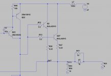
This is the output stage of my amplifier. I do not see any sign indicating any oscillation with 100nH in the wiring of the power suply source. Indeed, in a real prototype, there are 1uF plastic capacitors next to each transistor.
In my opinion, here, the problem is elsewhere, not in the output stage.
Attachments
I suspect with 1uF capacitors in the real circuit oscillations might be suppressed, but I'd probably use 1uF and an electrolytic too, locally (but this may give rise to half-wave signals as Douglas Self mentioned if not careful).
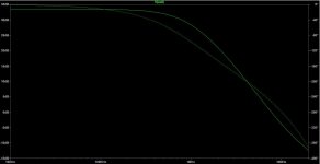
The problem is as ever a combination of all stages and the gain-phase relationship. My test was only to investigate whether the complementary style format is more sensitive than a straight "triple darlington". It may or may not apply to the circuit here, I have not entered that and simulated it but one post says it works. Your simulations only show the output stage in isolation, I think.
One output stage configuration may be more sensitive (i.e. less phase margin) than another when used with different front end stages, and whether they have power supply rejection (especially at high frequencies) etc. making the front end more sensitive to power supply leads.
Last edited:
In my test circuit adding 10 ohm emitter resistors to the first stage transistors and 2.2 ohms to the driver emitters suppresses the oscillations with the 100nH inductors in the supply line that I see. These are nominally 10% of the next stage base resistors and should reduce the local gain to 0.9 per stage compared with the previous values. In my view this makes them more like the straight triple gain stages. Just out of interest.
100% agree with you. My schematic from #68 post it is just output stage of a power amplifier. The simulations are made with all amplifier, not just outputstage in isolation. In that amplifier, the input stage it is CFP too. I simulated with 1uH in series with power supply and a nice solution to stop the oscillations it is a L//R circuit instead a base stop resistor.
A collection of stages under NFB is liable to have 180 deg of phase shift before the loop gain comes below unity.
The VAS cap must be large enough so it is "dominant", to give a 6dB/oct slope which is a 90 deg phase shift, all the way to unity loop gain (about 20 in power amps since we have 20:1 loss in the NFB resistors).
Do you mean cdom? What value is optimal?
Suggest adding small capacitors (100uF?) from rails to ground if the leads to the power supply are long, preferably on the output transistor collectors or as close to as possible.
They are indeed long, more than 1m. I'll try.
What is the maximum length of PS lines for not to exceed 100nH? Does it depend on thicknes of conductor?
I simulated with 1uH in series with power supply and a nice solution to stop the oscillations it is a L//R circuit instead a base stop resistor.
Would you please advise the values?
Last edited:
Andriy, due to some language barrier I can understand there may be a misunderstanding regarding the meaning of NPN-PNP-NPN or "triple" when discussing the output stage, when all are NPN it's also called "triple follower".
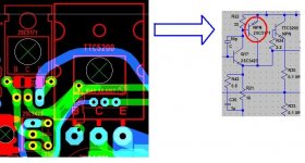
Due to many of us having different native languages it would be good if you first and foremost could start with numbering ALL components in your schematics in order to minimize misunderstandings, at least it seems the transistors are missing numberings, please correct it so people can point out directly any component on your schematics without having to describe with long and complicated sentences that may easily get lost in translation.
An the same with your PCB, add component numbering so people can help you debug it, it is the least to be asked for.
When it comes to your PCB design it seems the inconsistency is just continuing, this doesn't look good, just one example is the transistor arrangement around the CFP driver from your first post, see attached picture, there you have used an NPN transistor upside-down while it should be a PNP.
Also, you have been constantly fiddling and making small changes in your schematics, PCB design, and on your real amplifier without properly informing us what you are really doing, this if not right out dishonest to all members who are trying to help you, really embedding for serious misunderstandings and disaster.
As some others have mentioned, it would be a better and safer choice using triple follower instead of CFP in the driver stage, CFP really doesn't provide anything particular beneficial in This part of the amplifier, it may look cool and techy but in reality provides for more headache.
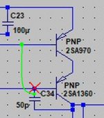
Also, C34 and C35 are connected wrong, they should be connected from cascode transistors collector to the other transistors base, see attached picture.
And one more thing, I already asked in your other thread (CFP Amplifier - Help Please!) where you have been troubleshooting your broken amplifier design for at least a half year, why do you need balanced input?
As far as I remember, virtually nobody have ever built it, the schematics with balanced input provided by lazycat was as far as I understood only a conceptual version of the single ended input version posted upon another members request, it seems simply not being a tested and verified design in real life.
Let's put it in clear language, do Not use balanced input unless you are going to use your amplifier in a specific environment that really really requires it, such as PA, otherwise please get over it!
There are probably several more questionable things, but this is now taking too much time to analyze in depth. When it looks like this, it is quite a hopeless project and quite impossible for the members on this board to help you with any further until you sort out all the mess, so again, let's go back to square one and begin with numbering all components in your schematics.
Due to many of us having different native languages it would be good if you first and foremost could start with numbering ALL components in your schematics in order to minimize misunderstandings, at least it seems the transistors are missing numberings, please correct it so people can point out directly any component on your schematics without having to describe with long and complicated sentences that may easily get lost in translation.
An the same with your PCB, add component numbering so people can help you debug it, it is the least to be asked for.
When it comes to your PCB design it seems the inconsistency is just continuing, this doesn't look good, just one example is the transistor arrangement around the CFP driver from your first post, see attached picture, there you have used an NPN transistor upside-down while it should be a PNP.
Also, you have been constantly fiddling and making small changes in your schematics, PCB design, and on your real amplifier without properly informing us what you are really doing, this if not right out dishonest to all members who are trying to help you, really embedding for serious misunderstandings and disaster.
As some others have mentioned, it would be a better and safer choice using triple follower instead of CFP in the driver stage, CFP really doesn't provide anything particular beneficial in This part of the amplifier, it may look cool and techy but in reality provides for more headache.
Also, C34 and C35 are connected wrong, they should be connected from cascode transistors collector to the other transistors base, see attached picture.
And one more thing, I already asked in your other thread (CFP Amplifier - Help Please!) where you have been troubleshooting your broken amplifier design for at least a half year, why do you need balanced input?
As far as I remember, virtually nobody have ever built it, the schematics with balanced input provided by lazycat was as far as I understood only a conceptual version of the single ended input version posted upon another members request, it seems simply not being a tested and verified design in real life.
Let's put it in clear language, do Not use balanced input unless you are going to use your amplifier in a specific environment that really really requires it, such as PA, otherwise please get over it!
There are probably several more questionable things, but this is now taking too much time to analyze in depth. When it looks like this, it is quite a hopeless project and quite impossible for the members on this board to help you with any further until you sort out all the mess, so again, let's go back to square one and begin with numbering all components in your schematics.
Attachments
Last edited:
No problem, I'll add numbering to the schematic. It could be more dificult with pcb, as there is not much free space, but I'll try.
I know about this silkscreen error in transistors arrangment, in input transistors as well. If the transistors would be used like on pcb, the amp won't work at all.
Sorry, but what I've done not informing about the changes? Do you mean new layout? it's only a project, not finished yet with pcbs.
I tried to connect C34, C35 in a way you showed, but without a change in oscillation.
As I remember I answered you why I would need balanced input. However it's not a problem here in the amplifier. It's working the same with SE input.
Last edited:
It's not so much thickness of the wire that matters for inductance, its the enclosed area, but the thickness will have a second order effect. If you use twisted pairs of wires, the enclosed area will be minimised, but on the other hand if you imagine a 100mm diameter loop the single turn has 300nH inductance which amounts to 150mm long wires if you think of them as connecting the PSU to the amplifier. But at >1m I definitely think you need to add local decoupling capacitors, but that might be a problem in itself as any ground leads will have quite a resistance, which, when a few amps flows, can induce millivolts which if sneak into the input could cause trouble. That is when you may find connecting the input earthy lead and the power ground lead together with a low value resistor (2 to 10 ohms) might stop oscillations. The resistance in this case needs to be high enough to stop circulating earth currents.
If you have not read any books on hifi layout and design I suggest it might help.
If you have not read any books on hifi layout and design I suggest it might help.
Last edited:
Andriyol,
Like I tried to tell you before, Ultima Thule explain you all issues concerning this project.
Please, compare the 'asc file' I sent you and you will find that the current sources in the Voltage Gain Stage are wrong. Add to this the error in the connections of Cdom capacitors and the decoupling capacitors that you put in wrong place near to 10R resistor you will have a impossible to work schematic.
Regards
Ronaldo
AndriyOL,
I suppose the best person to help you is Lazy Cat as he is the project owner and have total control of this project concept.
I also give you an simplified version of this concept that at least works in simulator. I recommend you to compare schematics and try to find a working circuit in simulator and after that you can go to an amplifier in real world.
I like to try different amplifier typologies and this one to not impressed me.
By the way, you have an old and really good Tektronix from good old times. I used one of this (7000 serie) in my very first project in electronic area in the beginning of 80's. Today I went to digital and use an DPO2024.
Regards
Ronaldo
Thank you Ronaldo for your advices.
I know LC is the best who can help here.
Btw, I tried to simulate the file you sent me, but prog tells some txt file missing.
Why don't you like this concept? because it's not working? Than which topology is your favorite and based on what specs you like it? For this won't be off topic, you can compare with current concept.
Thanks and Regards,
Andriy.
You are welcome.
I like the topology of Marantz MA700, but the compensation is not good in this module. You can find this topology in Onkyo M-504 and M-508 done in the best way it can be done. Technics used this same topology in a more complex schematics in old times.
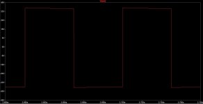
If you simulate square waves you find diferences in working beharviour
Here in forum the people call it the 'symasym' and there is very good examples in this forum (find OS schematics). He done a really DIY work with no intention of profile. This is my personal choice.
I changed the model files and you can simulate it now.
Have fun
Ronaldo
I like the topology of Marantz MA700, but the compensation is not good in this module. You can find this topology in Onkyo M-504 and M-508 done in the best way it can be done. Technics used this same topology in a more complex schematics in old times.
If you simulate square waves you find diferences in working beharviour
Here in forum the people call it the 'symasym' and there is very good examples in this forum (find OS schematics). He done a really DIY work with no intention of profile. This is my personal choice.
I changed the model files and you can simulate it now.
Have fun
Ronaldo
Attachments
Last edited:
- Status
- This old topic is closed. If you want to reopen this topic, contact a moderator using the "Report Post" button.
- Home
- Amplifiers
- Solid State
- One of the Top Solid-State CFA amp design