I would like you to know what would be getting before I post my simulation so I can look into any questions or matters arising.
There are a couple of tidying up things you could do - the component numbering and adjust the dc offset - now sitting at 46mv.
There is a discrete full complementary symmetry buffer feeding the alternative input since the input impedance at that point is low.
The buffer has a dc offset of -219 mV output so for simulation purposes I accepted this and put capacitors in series with the input and output.
This runs off plus and minus 32 volt rails that were available at the time of a earlier version that you were working with. The current draw is about 10 m.A.
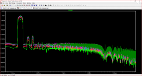
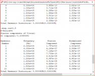
I have changed these to 40 volts as an afterthought to the data. The buffer THD can be seen by moving the vout label - taking this from the main amplifier output to a suitable spot after the buffer output cap.
I have measured the THD accordingly and attached the fft and some of the distortion results - practically non-extant with 40 volt rails. The buffer transistors are high voltage and the dissipation in the transistors is about 150 mW which is well within their ratings.
The main amplifier dc offset would normally be set by varying R8 and R9 which represent trim pots but a fine adjustment of a pot is not the same simple thing as changing a simulation resistor value. These "pots" also need to match the output halves to avoid spikes in the quasi LTP's.
How well the overall process goes I cannot say, but I think it will require some good hand skill and coordination.
To my mind it could be better to have a single trim pot elsewhere that can be used to set the dc offset such as at the buffer stage input.
I have not investigated this or the possibility of using a suitable IC for this job - probably the latter since these don't have significant dc drift.
I looked at changing the .models in the discrete buffer with 2N5401C and 2N5551C the suffix indicating Cordell models.
There is an include statement on one of my two simulations - to connect to Cordell's site so you can substitute that pair in the buffer to see what changes with dc offset.
With capacitor coupling this doesn't matter as far as the buffer THD and fft are concerned.
What this does to serve is to show how behaviour in simulations can vary depending on which versions of transistor models are used.
There are a couple of tidying up things you could do - the component numbering and adjust the dc offset - now sitting at 46mv.
There is a discrete full complementary symmetry buffer feeding the alternative input since the input impedance at that point is low.
The buffer has a dc offset of -219 mV output so for simulation purposes I accepted this and put capacitors in series with the input and output.
This runs off plus and minus 32 volt rails that were available at the time of a earlier version that you were working with. The current draw is about 10 m.A.
I have changed these to 40 volts as an afterthought to the data. The buffer THD can be seen by moving the vout label - taking this from the main amplifier output to a suitable spot after the buffer output cap.
I have measured the THD accordingly and attached the fft and some of the distortion results - practically non-extant with 40 volt rails. The buffer transistors are high voltage and the dissipation in the transistors is about 150 mW which is well within their ratings.
The main amplifier dc offset would normally be set by varying R8 and R9 which represent trim pots but a fine adjustment of a pot is not the same simple thing as changing a simulation resistor value. These "pots" also need to match the output halves to avoid spikes in the quasi LTP's.
How well the overall process goes I cannot say, but I think it will require some good hand skill and coordination.
To my mind it could be better to have a single trim pot elsewhere that can be used to set the dc offset such as at the buffer stage input.
I have not investigated this or the possibility of using a suitable IC for this job - probably the latter since these don't have significant dc drift.
I looked at changing the .models in the discrete buffer with 2N5401C and 2N5551C the suffix indicating Cordell models.
There is an include statement on one of my two simulations - to connect to Cordell's site so you can substitute that pair in the buffer to see what changes with dc offset.
With capacitor coupling this doesn't matter as far as the buffer THD and fft are concerned.
What this does to serve is to show how behaviour in simulations can vary depending on which versions of transistor models are used.
Attachments
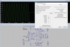
CFA input stage with true differential inputs using Rush pairs
The attached circuit shows a way to get true differential inputs using Rush pairs.
The discrete buffer is not required since the standard 4R differential opamp arrangement can be used for high CMRR.
The 4R diff amp assumes input sources are low resistance which is usually the case.

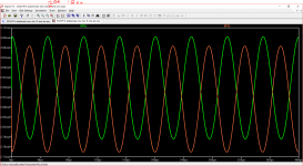
Plot below has +In and -In connected together.

Rush pairs can reduce the input offset voltage and currents when all the PNP's are the same batch and likewise the NPN's.
They are a variant of the LTP differential amp and can be thought of as an unfolded LTP, but does not need a tail source like the LTP.
The 10 ohm resistor between the two emitters of each Rush pair provides emitter degeneration just like the LTP.
To get ~10k input resistance on the inverting input then you can make R19 a T network to keep the feedback resistances low (~1k5).
There is a discrete full complementary symmetry buffer feeding the alternative input since the input impedance at that point is low.
The attached circuit shows a way to get true differential inputs using Rush pairs.
The discrete buffer is not required since the standard 4R differential opamp arrangement can be used for high CMRR.
The 4R diff amp assumes input sources are low resistance which is usually the case.
Plot below has +In and -In connected together.
Rush pairs can reduce the input offset voltage and currents when all the PNP's are the same batch and likewise the NPN's.
They are a variant of the LTP differential amp and can be thought of as an unfolded LTP, but does not need a tail source like the LTP.
The 10 ohm resistor between the two emitters of each Rush pair provides emitter degeneration just like the LTP.
To get ~10k input resistance on the inverting input then you can make R19 a T network to keep the feedback resistances low (~1k5).
Attachments
Perhaps parallel configuration resembles full complementary and phase symmetry is the way to go.
In that case I think we must thank Lazy Cat for his valuable advice. He is really a great designer. We only need to fine tune the schematic with enough phase margin within olg.
I tried to change input frequency in my sine wave sim from 1K to 20K, but it doesn't work that way.
What do you mean by the pots need to match output halves? As I know we can only choose the power rating, precision and number of turns in the pots.
Can we get the models of some Toshiba high ft bjts to closely match a performance in the sim of devices used on my pcbs?
If your simulations are satisfactory than the overall process should go the same.There is a discrete full complementary symmetry buffer feeding the alternative input since the input impedance at that point is low.
These "pots" also need to match the output halves to avoid spikes in the quasi LTP's.
How well the overall process goes I cannot say, but I think it will require some good hand skill and coordination.
I looked at changing the .models in the discrete buffer with 2N5401C and 2N5551C the suffix indicating Cordell models.
In that case I think we must thank Lazy Cat for his valuable advice. He is really a great designer. We only need to fine tune the schematic with enough phase margin within olg.
I tried to change input frequency in my sine wave sim from 1K to 20K, but it doesn't work that way.
What do you mean by the pots need to match output halves? As I know we can only choose the power rating, precision and number of turns in the pots.
Can we get the models of some Toshiba high ft bjts to closely match a performance in the sim of devices used on my pcbs?
Last edited:
The attached circuit shows a way to get true differential inputs using Rush pairs. <snip>
Ideas like this are a breath of fresh air.
Perhaps parallel configuration resembles full complementary and phase symmetry is the way to go.
If your simulations are satisfactory than the overall process should go the same.
In that case I think we must thank Lazy Cat for his valuable advice. He is really a great designer. We only need to fine tune the schematic with enough phase margin within olg.
I tried to change input frequency in my sine wave sim from 1K to 20K, but it doesn't work that way.
What do you mean by the pots need to match output halves? As I know we can only choose the power rating, precision and number of turns in the pots.
Can we get the models of some Toshiba high ft bjts to closely match a performance in the sim of devices used on my pcbs?
When the biasing of transistors relies on zener diodes and LEDs there can be small voltage variations. I have seen 1% zeners specified in some service manuals. Variations in mains voltage could be more than that.
The trim pots need to be set at around 47R so one of these could be a 1% resistor which then makes it a matter of adjusting only one trim pot of a value 100R.
If you are needing to adjust to a fraction of an Ohm that could prove to be finnicky. You could try a 10 turn cermet type if that will fit on your pcb, however you might also try an ordinary 200R trimpot with a 100R resistor soldered to the ends under the board.
The first attachment title suggests a 1khz simulation but the actual data is for 20khz so you can take and use these settings. The max step option for 1khz setting is on screen in blue - having been changed in status to comment. You can reinstate this by making this a directive and the equivalent for 20 khz a comment. You will have to change the data in other fields to show 1khz.
There are some other options for output SPICE models - I use those by Bob Cordell - you can find these by adding an include statement on the simulation and clicking browse viz .inc http://www.cordellaudio.com/book/Cordell-Models.txt
The circuit needs an output stability network and I have changed the output emitter resistors to those used in the Lazy Cat original with Iq where the voltage drop across these is optimum for low distortion at 26 mV. (Oliver criterion)
If 0.1R is substituted the standing current per device would need to be an inordinate 260 m.A.
Attachments
With these pots we can adjust biasing current and dc offset. With one pot it won't be possible.
Haven't you updated the schematic to differential VAS as LC sugested? Why did you set 60 V on front end PS and 40V on main PS? As I know minimum required difference is 5V higher on front end.
My circuit is stable with 0.1R emitter resistors, if I'm not wrong. There are other amplifiers with the same resistors working perfectly. I found base stoppers most stable optimal value is 2R
Last edited:
One of the problems with the original .asc file that has persisted through various changes is that every time one is made the circuit shrinks to an unrecognisable shape. Even when enlarged there is still a lot of fine detail where a 5 can look like a 6.
That said you can reduce the 60 rails in my simulation to 50 without prejudicing the stability. This will benefit the dc offset by reducing the level to 32 mV.
I suggest you check the distortion simulation with 0.1R emitter resistors at whatever Iq figure you set and compare the results given with my simulation and that you stick with 0.22R - not to mention thermal considerations.
There are two possible reasons for the 2 R resistors first these and the Miller capacitors around the first driver stage transistors were part of the stability
scheme.
This has to be achieved through one dominant pole and this was a rival to the main one - so I took it out.
The other possible reason for these resistors was to serve as fuses protecting the input stages if there was a short circuit of the output or if the output stage was over-driven into a low impedance load - possibly the purpose for which it was designed.
For normal use, supply rail 3-5 A fuses should be adequate protection.
Your original request was to get a working simulation of your dominant pole amplifier working preferably with the so called balanced components.
For me that was a matter of maintaining focus on the primary objective.
I am expecting to be absent from home either next week or the following one and will have no time to be looking at simulations. If you want to follow up on the suggestion by Lazy Cat just amend the circuit and give this a go and come back with your results.
You have not mentioned Ian Hegglun's ideas which have raised my interest - why not follow up on his lead in a new direction.
Do you mean to compare distortion with 0R1 and 0R22 in the same circuit? If the circuit won't be posiible to make it working with 0R1, than we have to use 0R22, no problem.
I'm using 3A smd fuses currently on pcbs.
Sorry, but Ian's idea is diffrerent from one already used in the circuit which appeared possible to make working. It requires implementation or a design of another circuit. It can be more complicated than properly compensate the current circuit. Also on the plot it seems inferior in performance than SSA input stage.
We will wait when you return to take a part in our research")
I'm using 3A smd fuses currently on pcbs.
Sorry, but Ian's idea is diffrerent from one already used in the circuit which appeared possible to make working. It requires implementation or a design of another circuit. It can be more complicated than properly compensate the current circuit. Also on the plot it seems inferior in performance than SSA input stage.
We will wait when you return to take a part in our research
The suggestion was to replace 0R1 with 0R22 and reset the Iq so the test is valid for the same Iq then look at the THD and compare the two results.
The purpose of emitter resistors is to inject a negative feedback voltage into the emitter to counter the voltage drop due to the element of series resistance (r'e) in the emitter diode.
With emitter resistor values of 0R1 that will be 260 mA at room temperature nominally 25 degrees C where r'e is 26 mV.
With three pairs of output transistors that will be 780 mA which will generate a lot of heat even with 50 volt supply rails.
If there is a rise in the transistor temperatures - for every 11 degrees C increase you can expect the conduction to double.
If you run the circuit at a lower current with 0R1 then the balance between the forward conduction diode voltage drop and that of the emitter will be out of check like moving the pivot point of a see-saw one way.
To quantify that, if you set your iq to 120 mA per transistor to match my setting the emitter resistor drop will be a mere 12 mV i.e. not congruent with 26mV in a push-pull sense.
The plot of Ian Hegglun's simulation is also below the 0dB gain level so as presented it attenuates.
More technical information http://www.hpl.hp.com/hpjournal/pdfs/IssuePDFs/1971-02.pdf
Author Bernard Oliver 2nd article see page 13 item (23) re emitter voltage drops.
Author Bernard Oliver 2nd article see page 13 item (23) re emitter voltage drops.
Actually the foregoing comments etc relate to the circuit with 60 volt rails but the pattern and THD figures are still representative.
I did not save the changes to these files when checking out the results of lowering the voltage rails to 50 volts last time round but I have rectified that now.
I did not save the changes to these files when checking out the results of lowering the voltage rails to 50 volts last time round but I have rectified that now.
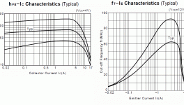
The characteristics or functions hfe(Ie) and ft(ie) are typical for power BJT with multi-emitter or ring emitter.Multi-emitter and ring-emitter power BJT specify the maximum fT. fT changes with collector current. It can be that a "high fT" power BJT has fT 30 MHz at Ic 2 amps but 100kHz at ic= 50 mA and ft 100 kHz at ic 8 amps. This holds also for base drive impedance close to zero. Makes compensation difficult . The original single diffused 2N3055 was rather easy to handle in terms of compensation as fT hardly varies with collector current
Aside or not: every musical instrument in general every sound source operates in time NOT in frequency domain . The engineering tool Fourier transformation which transform one domain into the respective other performs what the totality of auditive sense supposedly does it transforms a time series into what is perceived , a pitch tone a sound. But the physical reality of sound is time series, not frequency, and that is the reality of audio amps as well.
Attachments
Further sims
I have done more simulations on the simplified circuit to check this and it must be the case.
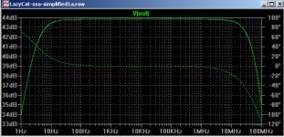
The attached circuit "1a" shows the AC plot when the second input "In-" is fed with an inverted signal wrt to the first input "Vin+". The gain reads 43dB in closed loop. (You would expect to feed an inverted signal to this input since it is marked "In-" in the original circuit by Lazy Cat).
Now open all the links to isolate the add-on parts to the 2nd input and the gain becomes 23dB. it's a huge difference in gain! You would expect the 2nd input to only add 6dB higher (double) with the second input added. So the second stage doesn't do what we expect it should.
The reason we can get this amp to "work" with the second input "In-" fed by the same noninverted signal is the gain is then 22.5dB in closed loop -- which is the same as that of the single input! So effectively the second input stage is "in neutral" and not contributing any gain. Which means it is could be removed since it works just as well without it provided both inputs are fed by the same signal. And it is a simpler circuit without the second input.
The second input is labelled as "Vin-", but it doesn't work as an inverting input, at least not over the voltage range that we want to use it for.
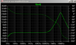
To show this I attached circuit "1b". It has 1k7 input attenuator added to the first input. Feeding with both inputs in phase we get -4dB (plot attached) and +43dB with the inputs out of phase.
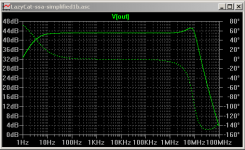
So we now have differential inputs? ... Yes and no. A .trans run shows the differential action only takes place for the first 10mV of the input signal range with gross distortion over most of the input signal range. So the second input stage doesn't do what we want.
And I can't find any simple way to modify the circuit to make it work with differential inputs over the full input voltage range of 1 or 2 volts. None of the suggested ideas work as differential inputs with the second input is driven with an inverted signal. Feeding the second input with a noninverted signal as mentioned) does not give the amp a balanced input at all.
The distortion is the proof that it doesn't work. Otherwise you must consider the distortion a feature. Who knows, maybe it will sound fine? But if you are comparing it to the amps it resembles, then the THD figure should indicate something has gone wrong.
The second input pair is shunting the feedback to ground resistor. Now all of the feedback current (which is a lot since this is a CFA) must be handled by the second input pair. It can't do his linearly. One proper solution would be to replace it with a very good buffer, an opamp would commonly be used like this.
Imagine a simple LTP amp. Add a 3rd transistor to the LTP and try to use it as a negative input. What happens? This is not exactly analogous to what was done here but it is the same kind of logical error.
I have done more simulations on the simplified circuit to check this and it must be the case.
The attached circuit "1a" shows the AC plot when the second input "In-" is fed with an inverted signal wrt to the first input "Vin+". The gain reads 43dB in closed loop. (You would expect to feed an inverted signal to this input since it is marked "In-" in the original circuit by Lazy Cat).
Now open all the links to isolate the add-on parts to the 2nd input and the gain becomes 23dB. it's a huge difference in gain! You would expect the 2nd input to only add 6dB higher (double) with the second input added. So the second stage doesn't do what we expect it should.
The reason we can get this amp to "work" with the second input "In-" fed by the same noninverted signal is the gain is then 22.5dB in closed loop -- which is the same as that of the single input! So effectively the second input stage is "in neutral" and not contributing any gain. Which means it is could be removed since it works just as well without it provided both inputs are fed by the same signal. And it is a simpler circuit without the second input.
The second input is labelled as "Vin-", but it doesn't work as an inverting input, at least not over the voltage range that we want to use it for.
To show this I attached circuit "1b". It has 1k7 input attenuator added to the first input. Feeding with both inputs in phase we get -4dB (plot attached) and +43dB with the inputs out of phase.
So we now have differential inputs? ... Yes and no. A .trans run shows the differential action only takes place for the first 10mV of the input signal range with gross distortion over most of the input signal range. So the second input stage doesn't do what we want.
And I can't find any simple way to modify the circuit to make it work with differential inputs over the full input voltage range of 1 or 2 volts. None of the suggested ideas work as differential inputs with the second input is driven with an inverted signal. Feeding the second input with a noninverted signal as mentioned) does not give the amp a balanced input at all.
Attachments
...Sorry, but Ian's idea is diffrerent from one already used in the circuit which appeared possible to make working. It requires implementation or a design of another circuit. It can be more complicated than properly compensate the current circuit. Also on the plot it seems inferior in performance than SSA input stage.
We will wait when you return to take a part in our research
The alternative input stage I have suggested could be used on your present PCB. It requires 4 extra transistors for the input stage.
Each of the input transistors Q2,Q3 will have Rush pairs and then there is the diode string of 4 biasing transistors which could go a a small matrix board.
Q6,Q7,Q8,Q9 reamain as current sources but different values for R8,R9. cascodes Q4,Q5,Q10,Q11 remain the same.
Compensation should be almost the same.
BTW I left the ccs and cascodes off my demo circuit because I was using the simplified form to demonstrate that it works and can give you differential inputs.
- Status
- This old topic is closed. If you want to reopen this topic, contact a moderator using the "Report Post" button.
- Home
- Amplifiers
- Solid State
- One of the Top Solid-State CFA amp design