I know one solution is to slow down the opamp stage. But that means less NFB available to suppress the quite nasty high-order crossover distortion from the CFP stage. So I would like to avoid that solution as much as possible.
First priority is a stable amplifier, and
NFB does not help much with crossover distortions.
Crossover distortions cause is that half of the AB output stage is cut off.
It takes a long time to build up the base-emitter charge and during this
time there is no NFB.
NFB will slew the preceeding amplifier stages into saturation during this time
in the worst case.
This causes more overshoot and limiting effects.
A good amplifier design starts with the output stage. The small signal
stages are not important in comparison.
Most output stages work, but very few have excellent impulse response
and current source/sinking capability.
CFP may not the best way for a capable output stage.
May be better to spent your time in a EF stage with active operating point
stabilization where no output transistor goes into cutoff.
Try to design for a single pole open loop frequency response.
Two pole compensation or TMC does not have good frequency and
impulse response, and nobody hears the difference
between 110 and 120 dB THD.
The snubber is important, because the CFP is a current feedback amplifier,I have not tested with capacitive loads yet, first it needs to be stable with a simple load resistor. I don't have an output inductor, but I do have a snubber although the ltspice schematic does not show it.
and the output impedance is important for the gain.
Base collector cap has a small current loop. Otherwise is see no difference.I will try and add a capacitor between base and collector of the driver transistor, since two of you have suggested it. Although I still don't see what the practical difference is between a base-collector capacitor or a base-ground capacitor. All the voltage swing is on the base, the collector is swinging almost no voltage.
It is a conservative number: Transitfrequency of output transistors dividedWhy should it be 500kHz of GBW? What is so special about that number? I'd like it to be as high as possible, while still keeping phase-margin high.
by 10.
Transitfrequency may be very low at 20 - 200 mA.
If it is stable with 500 kHz, you could try a higher number.
Keep us up to date from time to time!
Best wishes, Udo
Here is a gross misunderstanding about Class AB zero crossing.NFB does not help much with crossover distortions.
Crossover distortions cause is that half of the AB output stage is cut off.
It takes a long time to build up the base-emitter charge and during this
time there is no NFB.
NFB will slew the preceeding amplifier stages into saturation during this time
in the worst case.
This causes more overshoot and limiting effects.
It stems from confusion with class B and ambiguity about "Cross over".
A well designed class AB amp when zero crossing actually works as a Class A amplifier, there is none of the scary phenomenons you are mentioning ( no NFB, slewing, base charge buil up and the like ) Those belong to Class B.
In a Class B the crossing zero scenario is: One leg ON, None ON, the other leg ON. With the dreadful cross over distortion, where NFB cannot help at all.
In a Class AB the crossing zero scenario is: One leg ON, Both ON, the other leg ON. With a more confortable distortion from gm doubling, that is efficiently lowered by NFB.
With this, well understood about Class AB, one can debate about how wide the Class A region should be.
This is more a matter of opinions, some like it wide, some like it narrow, some believe in Oliver optimum.
Related is EF for big endians and CFP for little endians.
In the static DC case you are right.
In the typical dynamic case the power transistor base charge has to be build-up fast.
At the same time the complementary power transistor is switched off, and his base charge has to be removed.
Both processes are relativly slow and result in base current spikes, which
are sourced by the driver stage.
NFB tries to correct the resulting errors, and as a result the driver
transistor base slews somewhat (surely not up to the rails!).
If this would not be the case, no high frequency crossover distortion
would happen (as in class-A, where no significant base charge has to be build up or removed).
The new CFP PCB from Seeed is finally here! Two weeks from Seeed to Norway, and another two weeks through customs processing by the postal service... 
Anyway, moved all the parts over from the previous CFP effort, using BD139/140 as drivers, soon ready to turn it on. Stay tuned!
Anyway, moved all the parts over from the previous CFP effort, using BD139/140 as drivers, soon ready to turn it on. Stay tuned!
Attachments
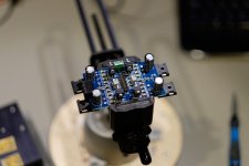
I'm just using a regular old soldering station. The PCB is 50x80mm. This is just the output stage, drivers and output transistors and Vbe multiplier. The opamp stage is on a separate PCB that plugs into the pin header. I'm very pleased with this modular approach, allows easy testing of different input and output stages.
And the results are in!
Unfortunately, it's disappointing. The BD139/140 drivers needed 100p CB caps and 22R base stopper resistors in order to become stable...
The THDN results then became exactly the same as those in post 54.
So a lot of work for no improvement, but I'll chalk it up as a learning experience. It's a shame because the CFP really excels in one department: Keeping a very stable idle current! No matter how warm the amp is, the idle current immediately settles to the correct value.
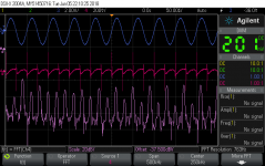
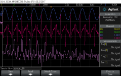
So I am going back to the EF output stage from here on in my quest for linearity. The reason is shown quite clearly in these 'scope captures:
Trace 3 and 4 is the monitor output and the distortion residual respectively from the AP1. The signal is 20kHz/10W/8ohm and the analyzer bandwith is set to 500kHz.
scope_10.png is with the EF output stage and scope_20.png is with the CFP output stage. Note the different scale of trace 4, the distortion residual! The math trace shows the FFT of the distortion residual with 50kHz/div. All the high order harmonics resulting from crossover distortion in the CFP stage is quite something...
Unfortunately, it's disappointing. The BD139/140 drivers needed 100p CB caps and 22R base stopper resistors in order to become stable...
The THDN results then became exactly the same as those in post 54.
So a lot of work for no improvement, but I'll chalk it up as a learning experience. It's a shame because the CFP really excels in one department: Keeping a very stable idle current! No matter how warm the amp is, the idle current immediately settles to the correct value.
So I am going back to the EF output stage from here on in my quest for linearity. The reason is shown quite clearly in these 'scope captures:
Trace 3 and 4 is the monitor output and the distortion residual respectively from the AP1. The signal is 20kHz/10W/8ohm and the analyzer bandwith is set to 500kHz.
scope_10.png is with the EF output stage and scope_20.png is with the CFP output stage. Note the different scale of trace 4, the distortion residual! The math trace shows the FFT of the distortion residual with 50kHz/div. All the high order harmonics resulting from crossover distortion in the CFP stage is quite something...
Attachments
- Status
- This old topic is closed. If you want to reopen this topic, contact a moderator using the "Report Post" button.
- Home
- Amplifiers
- Solid State
- Bridged Buffered Opamp Amp - a journey