That's cheating, the amplifier is still producing the harmonics. The filter just reduces the proportion in the output after the filter.................
An inductor to cut at 80KHz 3dB will give you a substantial improvement of THD20.
You already have 0.0005%. With the inductor, I guess-estimated you can expect 0.0002%.
If one is designing and building to be a low THD20, then you measure before the filter.
Andrew you missed the part about the inductor being a part of the zobel. Nuts and bolts parts. Plus, let's not talk about applicability of thd at 20k, as it's definitely not total with 80k sampling, nor is there anyone out there to hear it. 19+20 IMD sure, good test to measure upper band performance (or higher frequency input imd I'd you want to see ultrasonic linearity.
Just a quick note to all of you following this thread, I'm still here! Your comments and the discussion is highly appreciated!
I am thinking about improvements and how to make it even better, but without the design becoming too complex. The simplicity and low component count of this amp is appealing to me.
I am working on improving both the input and the output stage, increasing loopgain of the former and improving linearity of the latter. Perhaps I have something to share next year, but now the holiday starts! Merry X-mas to you all!
Hi, thank you for not forgetting this thread!
I have actually done quite a bit, but I don't have any really improved results to show for it, so that's why I haven't posted anything.
I guess it's worth posting also what I have tried that _didn't_ work out, so I'll consider doing that from now on.
Firstly, what didn't work out as well as I had hoped was the SMT driver transistors. The reason I wanted to try it was that there are some very nice high-speed transistors in SMT packages, so I wanted to try it to make a high-BW output stage. I've tried different types in SOT-223 and SOT-89 packages, and they work well as long as the supply voltage is kept low, but when the supply voltage goes above 30V or so, so they fail. SOA limit I suppose.
So I decided to try something very different, a output board with the Sanken STD03 transistors.
I couldn't abandon the SMT driver idea completely though, so I have also made a CFP output stage using PHPT610030NPK transistors for driver and Vbe multiplier.
Both output stage PCBs are currently on its (slow) way with Hong Kong Post.
I have tried another more complex input stage, and it seems to possibly give even lower distortion, but as I am already at the limit of my AP1, it's hard to say. To make any progress here I have finally ordered a Cordell DM from Pilgham Audio, and it should arrive this month as well. I think it'll be a great companion to the AP1.
Very interesting. This is a lot of hard work.
About a Vbe multiplier for base spreading of a CFP output stage, what about this alternative: Using diodes, two PHPT610030NPK, one of them as driver transistor and diode at the positive side, the other one as driver transistor and diode at the negative side. The idea is thermal tracking of drivers and base spreaders. Biais adjust of this output stage would be adjusting the current supplied by two CCS from rails to the diodes and drivers bases.
About a Vbe multiplier for base spreading of a CFP output stage, what about this alternative: Using diodes, two PHPT610030NPK, one of them as driver transistor and diode at the positive side, the other one as driver transistor and diode at the negative side. The idea is thermal tracking of drivers and base spreaders. Biais adjust of this output stage would be adjusting the current supplied by two CCS from rails to the diodes and drivers bases.
Yes, you are close. I choose to do the Vbe multiplier like version C here, with one half of the transistor being the driver, and the other half being one of the Vbe transistors.

Should give very close thermal tracking. It can turn out to be too close though, then the bias will follow the signal envelope... Time will tell...
Should give very close thermal tracking. It can turn out to be too close though, then the bias will follow the signal envelope... Time will tell...
I like C.
With
_a second CCS at the V- ( instead of the bottom transistor )
and
_the op-amp output at the Vbe mutiplier mid point ( the two emitters )
The two CCS do not need exact current matching, the current difference will be taken care of, by the op amp output current.
This gives a minimal power from the op-amp. This gives an excellent PSRR.
I like symmetry, may be that is just cosmetics. -: )
Interesting little project and very good measurement results.
Regarding your conclusions i am not of your opinion.
My humble comments:
=>6: You have roughly doubled the cost of a typical amplifier.
You need two specialized high voltage opamps with high GBW
to replace 6 small signal $0.05 transistors of a typical
single ended amplifier.
Additionally you need TWO output buffers with expensive transistors.
And power is still limited to about 50 Watt.
=>5: This is not a High GBW amplifier as the typical gain of a power
Amp is about 20.
Therefore the 50 MHz of the opamp results in 2.5 MHz GBW of your
bridged amplifier.
The loop gain is only 125 at 20 kHz and this is the reason that
you have no stability problems.
=> 4: Almost any $0.05 transistor with reasonable high beta,
which is running at 1-2 mA, has lower voltage noise.
=> 3: Is the same for discrete Amps.
=> 2: True, but not important as the feedback network has low
value resistors.
=> 1: It is easy to achieve less than 5 mV DC offset in a discrete
amplifier, and you cannot leave out AC coupling, as it safeguards
your amp from faulty equipment.
So i do not see a single argument in favour of the bridged opamp amplifier
configuration.
But it shows that amplifier design is no magic art, and that many
ways lead to good (neutral) sounding amplifiers.
Thank you.
Yes I think an opamp as an input stage has many benefits:
1. Low input offset voltage and no offset drift means you can avoid servos and AC-coupling capacitors and offset adjustment pots.
2. Low input bias currents means less constraints on resistors for input and feedback network.
3. No low frequency oscillation.
4. Low voltage noise and/or current noise without needing exotic transistors.
5. High GBW.
6. Low parts count.
The only drawback is the limited output voltage swing from most opamps.
So the only main non-linearity I am left with now is that of crossover distortion from a class-B output stage.
The thermal stability of my amplifier is pretty good but not perfect. I am using just a standard Vbe multiplier with the Vbe transistor on top of one of the output transistors. Since it's a bridged amp, there are two pots that need to be adjusted and kept in sync, that is a minor drawback.
I have taken some interest in autobias/sliding-bias output stages, I've done some simulations of existing designs but not found any that I am really happy with yet.
I see that I promised some plots earlier of THD vs various bias currents, that is coming up soon.
Hi udok, thank you for your interest.
6: My original claim was not low cost, but low parts count. Not quite the same") You are probably correct that a single-ended amplifier with discrete transistors would be cheaper. However my amplifier is 90W/8ohm, 160W/4ohm, and to get the same SOA in a single ended amplifier of the same rated power, you would still need double output devices, I think.
You are probably correct that a single-ended amplifier with discrete transistors would be cheaper. However my amplifier is 90W/8ohm, 160W/4ohm, and to get the same SOA in a single ended amplifier of the same rated power, you would still need double output devices, I think.
5: For a one-pole amplifier the GBW is independent of the closed-loop gain. So the GBW is still 50MHz. In terms of audio power amplifiers that is higher than usual GBW I think. And, as I stated in one of the posts, the amplifier is stable at 6dB gain in each leg of the bridge. So by the same calculation bandwidth (not GBW) is then 25MHz, and loopgain at 20kHz is 1250 (~60dB). A simple op-amp based preamp could be added to get the total gain up to the common value of 26dB.
4: Perhaps, but the input stage would need degeneration to improve linearity and then noise would increase. I think opamps are hard to beat for the combination of linearity and noise.
3: I agree, with thermally coupled input transistors this isn't usually an issue.
2: Yes, but with higher bias-currents you still need to be careful about matching impedances on both sides of the diff-amp input stage.
1: I agree, AC-coupling is a nice safeguard. But it's nice to have the possibility to run DC-coupled if you have control of your signal chain, as most of us DIY'ers do.
So I still think there are some benefits, but there are always some tradeoffs as well.
6: My original claim was not low cost, but low parts count. Not quite the same
You are probably correct that a single-ended amplifier with discrete transistors would be cheaper. However my amplifier is 90W/8ohm, 160W/4ohm, and to get the same SOA in a single ended amplifier of the same rated power, you would still need double output devices, I think.5: For a one-pole amplifier the GBW is independent of the closed-loop gain. So the GBW is still 50MHz. In terms of audio power amplifiers that is higher than usual GBW I think. And, as I stated in one of the posts, the amplifier is stable at 6dB gain in each leg of the bridge. So by the same calculation bandwidth (not GBW) is then 25MHz, and loopgain at 20kHz is 1250 (~60dB). A simple op-amp based preamp could be added to get the total gain up to the common value of 26dB.
4: Perhaps, but the input stage would need degeneration to improve linearity and then noise would increase. I think opamps are hard to beat for the combination of linearity and noise.
3: I agree, with thermally coupled input transistors this isn't usually an issue.
2: Yes, but with higher bias-currents you still need to be careful about matching impedances on both sides of the diff-amp input stage.
1: I agree, AC-coupling is a nice safeguard. But it's nice to have the possibility to run DC-coupled if you have control of your signal chain, as most of us DIY'ers do.
So I still think there are some benefits, but there are always some tradeoffs as well.
used very similar setup in 80's with LF353 driving IRFZ40 , IRF9Z40 transistors in a small case for car stereo use. A 555 timer was used to boost op amp voltage to 20v and -7 volts to drive bias and FETS to high current levels. Distortion of less then .01% at 20w output.
Dc output voltage is 1/2 battery voltage.
Dc output voltage is 1/2 battery voltage.
Update!
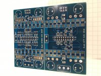
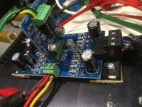
Received PCBs from Seedstudio finally. This is both the CFP and the STD03 based output stages. I have the parts for the CFP stage, but not sure when I will have the time to solder it up, busy both at work and at home this month.
Also I don't have high hopes for the CFP stage, it oscillates in LTSpice no matter what I do...
The Cordell DM I ordered from Pilgham Audio has still not arrived, hopefully it's just bad luck.
Attachments
Thanks for the update.
This is bad news about CFP.
I have no stability issue whatsoever with LTspice on a op amp design with LT6090 and CFP with Toshiba 2SC5200/2SA1949 TTA004/TTC004. Models from LT and Toshiba. With large capacitive load it does need an output inductor to go back stable, with simulated inductive tracks base stoppers do restore stability.
I understand about such topology that, for stability, the current booster needs a faster Ft than the op amp. What about Ft of the driver bjt versus the output bjt ? I am confused about this but think that is the key for stability of an op amp with CFP. What do you think ? Should we have FT of op amp < driver < output, OR, op amp < output < driver.
Have you tried caps at c.b. of drivers to decrease their effective Ft ? Then may be the op amp is too fast.
To be honest, I do not understand well enough CFP stability and wish all helps and comments about this.
Finally an update!
I have assembled and tested the CFP output stage. And my fears came through, it oscillated like crazy in the beginning.
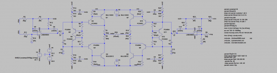
After lots of experimentation on compensation I ended up with a RC filter (22R/470p) between the opamp and the output stage in addition to usual TMC compensation (10p/4k/10p).
This throws away quite a bit of loopgain compared with the EF output stage.
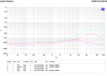
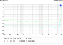
This shows in the measured THD as well. Although it's below the measurement floor for frequencies <1kHz, it rises above that and ends up at 16-20ppm at 20kHz.
That number may still be ok, but what worries me is the distribution of the harmonics. Lots of high-order harmonics due to a very sharp discontinuity at the crossover.
The textbooks and simulations predicted this, but I didn't think it would be this bad in practice, but it is. So the CFP seems to be a dead-end, unless someone has a good tip for me on how to "fix" it.
I have assembled and tested the CFP output stage. And my fears came through, it oscillated like crazy in the beginning.
After lots of experimentation on compensation I ended up with a RC filter (22R/470p) between the opamp and the output stage in addition to usual TMC compensation (10p/4k/10p).
This throws away quite a bit of loopgain compared with the EF output stage.
This shows in the measured THD as well. Although it's below the measurement floor for frequencies <1kHz, it rises above that and ends up at 16-20ppm at 20kHz.
That number may still be ok, but what worries me is the distribution of the harmonics. Lots of high-order harmonics due to a very sharp discontinuity at the crossover.
The textbooks and simulations predicted this, but I didn't think it would be this bad in practice, but it is. So the CFP seems to be a dead-end, unless someone has a good tip for me on how to "fix" it.
Attachments
Hi,
Yes I believe the Vbe multiplier is ok, although I know the collectors of the Vbe transistors do not have a well-define voltage.
Actually the idle current is one of the things that is very good with this CFP stage. It is very stable, and settles quickly to the correct value after a transient.
Also a nice feature of the CFP is that the optimal bias current is lower than the EF stage, and so it runs very cool. Just 0.1A idle supply current for the whole amp.
"You switch the transistors between them." Not sure what you mean here, want to explain some more?
I believe R17 and R32 works as base-stop resistors. I also tried adding resistors (10ohm) to each driver base, but that was not enough to prevent oscillation.
Perhaps, as mchambin points out, that the CFP stage works better with slower driver transistors. I think we need FT of op amp < driver < output.
You can try adding miller (C-B) caps to the CFP. First try drivers, then try o/p's... No guarantees.
For the sim imho start with just the "one half" and get it straight first.
Also I would delete the R12 at the beginning. Add it back in when you get the whole o/p stage to behave.
For the sim imho start with just the "one half" and get it straight first.
Also I would delete the R12 at the beginning. Add it back in when you get the whole o/p stage to behave.
You can try adding miller (C-B) caps to the CFP. First try drivers, then try o/p's... No guarantees.
In my head the caps from driver base to ground achieves the same thing, but perhaps I am mistaken? There is very little signal swing on the drivers collector, so connecting the capacitor from base to collector, or base to ground is almost the same thing? I'd be happy to hear an explanation of why there is any significant difference.
Of course, I only sim one half of the amplifer for stability.For the sim imho start with just the "one half" and get it straight first.
Of course, I did.Also I would delete the R12 at the beginning. Add it back in when you get the whole o/p stage to behave.
I guess that the 470pF - 22R filter is bad idea as it adds
phase to the output stage.
Your problem is a very fast opamp stage which drives
a slow output power stage.
The opamp sees an error and tries to correct it,
but the slow output can not follow in time,
and the opamp is shooting over the goal.
The solution is to make the opamp stage slower.
Try to avoid TMC for the start and leave out R12 and C6 in
the feedback.
Increase the very small 10 pF to 100 pF and make some
tests with a fast rising pulse.
The 100pF between opamp output and negative input
builds an integrator and this slows down the opamp stage.
Do some tests with fast rising pulses and capacitive loads.
I would guess that you get more troubles as you have
no isolating inductor at the output and no snubber.
An output capacitive load together with the open loop
amp output resistance is a R-C filter, which adds phase.
A good amplifier has zero overshoot.
For audio purposes, a bessel filter with constant group delay
may even be preferable.
The problem with the CFP is that it is really a small inverting amplifier
with gain. Here you have a similar probem: a fast driver
transistor and a slow output transistor.
Try to add a Miller C between the Collector and base of the driver...
Your amplifier is a cascade of two stages:
The opamp stage should be designed to have unity gain frequency of
about 500kHz (= -90 degree of phase).
The output power stage (with gain of 1) should not add more than about
-45 degree at 500kHz.
This would give you a small overshoot as in a Butterworth filter.
You can test the opamp driver and the output driver in isolation.
Each should be stable in isolation. the output stage should not add
more than 45 degree of phase at the unity gain frequency of the
opamp stage.
Good Luck,
Udo
Last edited:
Hi udok, thank you for the long and useful reply.
I agree with most of your analysis, it is a fast opamp driving an output stage which in itself is a 2-stage amplifier with feedback using fast input transistor and comparatively slow output transistors. It's a configuration asking for trouble.
I know one solution is to slow down the opamp stage. But that means less NFB available to suppress the quite nasty high-order crossover distortion from the CFP stage. So I would like to avoid that solution as much as possible.
I have not tested with capacitive loads yet, first it needs to be stable with a simple load resistor. I don't have an output inductor, but I do have a snubber although the ltspice schematic does not show it.
I will try and add a capacitor between base and collector of the driver transistor, since two of you have suggested it. Although I still don't see what the practical difference is between a base-collector capacitor or a base-ground capacitor. All the voltage swing is on the base, the collector is swinging almost no voltage.
Why should it be 500kHz of GBW? What is so special about that number? I'd like it to be as high as possible, while still keeping phase-margin high.
Here are my notes from the different compensation variants I have tried so far:
47p MC + no LPF + 0R RB -> oscillation
47p MC + 22R/470p LPF + 0R RB -> stable
22p/4k TMC + 22R/470p LPF + 0R RB -> stable
10p/4k TMC + 22R/100p LPF + 0R RB -> oscillation
22p/4k TMC + 22R/100p LPF + 0R RB -> oscillation
22p/1k TMC + 22R/100p LPF + 0R RB -> oscillation
10p/1k TMC + 22R/100p LPF + 0R RB -> oscillation
10p/1k TMC + 22R/470p LPF + 0R RB -> stable -> 0.00400% THD+N at 20kHz/10W/80kBW
10p/NU MC + 22R/470p LPF + 0R RB -> stable -> 0.00220% THD+N at 20kHz/10W/80kBW
10p/4k TMC + 22R/470p LPF + 0R RB -> stable -> 0.00160% THD+N at 20kHz/10W/80kBW
10p/10k TMC + 22R/470p LPF + 0R RB -> stable -> 0.00160% THD+N at 20kHz/10W/80kBW
5p/10k TMC + 22R/470p LPF + 0R RB -> oscillation
5p/2k7 TMC + 22R/470p LPF + 0R RB -> oscillation
10p/2k7 TMC + 22R/470p LPF + 0R RB -> stable -> 0.00160% THD+N at 20kHz/10W/80kBW
Testing the opamp and output stage in isolation is a good idea, I'll try that.
While playing a little with the spice simulation I discovered that with the old BD139/140 from Cordell's models, the amp was stable without any 22R/470p LPF. So I decided to make a variant of the output board with TO126 drivers. Sim with the MJE340/350 models oscillated again, so it might not be big success. We'll see.
The design is sent to Seeed so they can make it while I'm on summer vacation. The weather has been exceptionally nice here this summer so it means spending time outdoors is prioritized higher. It might therefore be a while until the next update.
- Status
- This old topic is closed. If you want to reopen this topic, contact a moderator using the "Report Post" button.
- Home
- Amplifiers
- Solid State
- Bridged Buffered Opamp Amp - a journey