Dosen‘t seem like theres any plorbem
Thermal stability can be fixed by placing q11 onto same heat sink as q14 q15 are mounted on
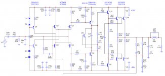
However main concern for you is over biasing for your voltage gain stage 2sb 649.
Maximum power through transistor approximated to be half of vcc divided by emitter resistance times half of vcc
which means (15/47)(15)= 4.785W of power disiplatio. unless your vas is heat sinked it will die .
For your first design, highly recomended that you play at lower power for you gain stages, then step up the bias after you tested the first one to be working.
I would also recomend the collector resistors of the diffrential pair to all be the same values.
Approximation of idle bias for your vas is about 30-(3.3/2)(820)= voltage appearing at base of q7.
Voltage at emitter = vb-0.6 = approx0.765v
0.765/47*29v= approx470mW of quisent. This is half of maximum disipation without heat sink for vas. it will run boling hot.
Thermal stability can be fixed by placing q11 onto same heat sink as q14 q15 are mounted on
However main concern for you is over biasing for your voltage gain stage 2sb 649.
Maximum power through transistor approximated to be half of vcc divided by emitter resistance times half of vcc
which means (15/47)(15)= 4.785W of power disiplatio. unless your vas is heat sinked it will die .
For your first design, highly recomended that you play at lower power for you gain stages, then step up the bias after you tested the first one to be working.
I would also recomend the collector resistors of the diffrential pair to all be the same values.
Approximation of idle bias for your vas is about 30-(3.3/2)(820)= voltage appearing at base of q7.
Voltage at emitter = vb-0.6 = approx0.765v
0.765/47*29v= approx470mW of quisent. This is half of maximum disipation without heat sink for vas. it will run boling hot.
Last edited:
Member
Joined 2009
Paid Member
The challenge with this circuit is keeping a stable current flow through the VAS, Q7,9, as temperature variations will affect their operating points. The use of R7 and R10 helps quite a bit, I made a circuit like this but with much higher degeneration on the VAS for better stability. With current variations through the VAS you also get variations in bias for such a simple Vbe multiplier (Q11). This too can be improved using the Hagerman circuit. What I did is shown here:TGM5 - all-BJT Simple Symmetric Amplifier
I was never that happy with the sound.
I had significantly better results with this one:TGM7 - an amplifier based on Greg Ball SKA
I was never that happy with the sound.
I had significantly better results with this one:TGM7 - an amplifier based on Greg Ball SKA
pretty straight forward double diff, push pull VAS. degeneration of the LTP might be good. Med power VAS is not always a bad thing if designed properly but I believe it limits the components as far as specs go, that are available for such an operation. It all depends on the output stage for that.......which is a different subject.
I recomend that R7 R10 stays at 470 ohms for the first prototype build. Everything else can be kept same and should work
You'd also want to adjust vbe multipleier at lowest current first, something like equal emitter and collector resistance for lowest biasing, once working and sound, you then adjust bias and play arround.
You'd also want to adjust vbe multipleier at lowest current first, something like equal emitter and collector resistance for lowest biasing, once working and sound, you then adjust bias and play arround.
for d1 to d4 you can replace them with zener diodes, typically 2.4v to 4.7v is recomended. Larger voltage means biasing of diffrential pair changes less due to missmatching of transistors and resistors.
Voltage through r1 r2 can be estimated as zener voltage minus transistor be voltage assumed to be approx 0.6 to 0.7v.
this is the total current through q2 q3.
The current through just q2 estimated to be half of total current.
example 4.7v zener, voltage accross r1 estimated to be 4.7-0.6= 4.1v.
V=IR, because voltage is constant through r1r, the current will be popotional to current.
if r1 is 1k ohms this means the total current through q5 q6 is 4.1/1000= 4.1mA
The current through individual transistor q5 estimated to be half of 4.1mA = 2.05mA.
Because current is fixed you can then estimate the voltage drop from collector resistor.
Lets say you use a 2k2 resistor for Collector.(r5 r41)
the voltage accross 2k2 would be 2.05mA times 2200ohms=4.51V
This means the voltage accross R10 is estimated to be 4.5v-vbe drop of q9.
vbe approx 0.6v
this means 3.9v will be droped accrosed r10.
From there you can estimate idle current of q9 and detrimine heat sinks and resistor value of r10.
Maximum power consumpotion of resistor and q9 can be estimated
this is half of supply voltage divided by the value of r10. This tells you the current through r10 and q9.
From there you know current and volt drop accross q9 r10 is approx half of supply voltage. you can calculate maximum power disipation.
When you output approx 15v pk-pk sine wave the maximum power accross r9 would be this number
EDIT: Large zener diode values means if your diffrnetial pair needs lots to output a large voltage, your maximum voltage swing will be reduced. However mostcases this voltage swing is low because the following stage does most or all of the amplification.
Estimation of maixmum power example r10 is 470ohms, current would be 15/470=0.0319A
maximum power through q9 approx 0.0319*15 = 0.4785w
By the way this assumes r38 r39 are short circuited and all diffrential pair are directly suppled by vcc
Last edited:
Just wondering about the position of the shunt compensation. In this amp it is on the base of the VAS transistors. Normally the shunt compensation is the collectors of the VAS transistors. Not tried simulating the stability of this design so may work ok. But at present the VAS may be excessively affected by the varying load of the driver transistors as this is the only loading. So just asking the question.
Paul
Paul
Thx all.
I think about some LED diodes, maybe lower noise.
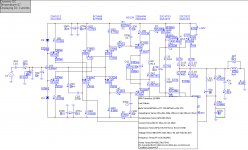
Stability in simulation looks good, but need trim few capacitors. 140° phase shift is chalenging. I make some pic.
mcd99...please post some picture with this compensation.
smy14inch...thx, i try this
R38,39 i try better PSRR. Any idea other way?
last try, phase 150°
https://i.imgur.com/wXBcEGg.jpg
I think about some LED diodes, maybe lower noise.
Stability in simulation looks good, but need trim few capacitors. 140° phase shift is chalenging. I make some pic.
mcd99...please post some picture with this compensation.
smy14inch...thx, i try this
R38,39 i try better PSRR. Any idea other way?
last try, phase 150°
https://i.imgur.com/wXBcEGg.jpg
Last edited:
You can still have r39 r38, all this means is the voltage ce of your diffrential pair decreases slightly. Current stays the same with or without r39.
The collector drop woulod also be affected slightly this means vas has slightly diffrent current than calculated.
voltage appearing at accross r10 estimatd to be current through q6 times r5.
Plus ((q5+q6 current) times r39).
For phase shift plorbem, try removing c9,c18,c1,c3,c5,c11,L1,c8
when music playhing currtent of diffrential pair is changing, r39 r38 has capacitor connected parallel to ground, this may cause phase shift, try removing c12 c14 etc. Or try removing r39 r38
This means ac signal which will try to appear at r39 r38 when music is playing becomes grounded by c12 c14.
From my point of view r39 r38 decreases sound quality, therefore it is not recomended.
For better ripple rejciton I recomend c7 to be 330-470uF. I have used 470uf and 680 ohms for r17 without any plorbem. However more capctirance for c7 amplifier error will occur and self destruct. Higher resistance r17 means better rejection, but c7 must be smaller
Last edited:
From your original circuit, I don't see any reason for phase shift to occur. Maybe its the circuit simulator giving you the wrong results.Yes. R38,39 raising THD, but solo capacitor is not good for clean power. RC is better, or not? But ok. I kick this out. resistors and elyts. Original circuit is without this.
from the picture of circuit simulator you have no phase shift up untill 200khz.
Audio specturm 20-20khz only.
This is absolutley normal. As expected you do not have any phase shift error and orignal circuit will work.
EDIT:just an idea for less noise. You can regulate only your drivers and leave output transistors unregulated. Something like a lm317 337 would work without a heat sink. vin vout diffrential voltage can be set 2v to 3v.
If you do do this make sure you bypass the adjustment pin, otherwise dosen't reduce noise at all from my exprience
Last edited:
I think you need to change some values and the design.
This is symmetrical amplifier and i think for stability and good performance you need to change:
R4,R5,R40,R41 = 1K
R32,R33,R38,R39,R42,R43 = Not need put 0R
Change the place of C1+R8 to Q7 B-C (not B-E) also at Q9
R34 and R35? for what 2 resistors? 1 resistor of 220R between the Q8,Q10 Emiters
C11? No need


- Status
- Not open for further replies.
- Home
- Amplifiers
- Solid State
- AB amplifier, first try